Basic Audio Amplifier
CIRCUIT
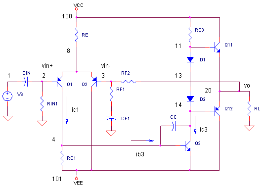
BASIC_AMPLIFIER.CIR Download the SPICE file
Let's explore the basic DNA of an audio amplifier. This internal structure not only describes the majority of audio amps today, but also the innards of most op amps today. The design of these amplifiers share 3 common building blocks. Designers optimize the gain, linearity or power in various stages depending on the requirements - from a cheap headphone amplifier to a high performance 100W sound system. And this gives rise to the vast number of different types of audio amplifiers and op amps running around the universe today. We'll build an audio amplifier and follow the signal through the structure. Finally, you'll get a chance to vary components to see their effect on performance.
By the way, there's enough literature on the design and analysis of audio amps to choke a horse. We'll try to hit the essential points. The basic amplifier above is a great place to start. But wait, there's more! In other topics, we'll explore each stage and enhance it. With the help of some hands-on SPICE simulations, you'll understand every component, its role, and how to make a reasonable design choice about it.
THREE BUILDING BLOCKS
In a nutshell, here's the three fundamental building blocks of audio amplifiers (and op amps).
| Stage | AC Signal Equation | Description | |
|
Differential Input Stage Q1,Q2 |
ic1 = 1/2 · (vin+ - vin-) · gm |
A differential input is
required. Why? We use feedback to control the amp's gain. The term
"feedback" implies we drive the positive input vin+ and feedback some of
the output (using RF1, RF2) to the negative input vin-. This is also a trans-conductance stage: voltage in, current out. The transconductance gm1 of Q1, Q2 set the gain of this stage. Unfortunately, the output is a current! No problem, the next stage gets us back to voltage. |
|
|
Gain Stage Q3 |
vc3 = ic1 · Ki · beta3 · RC3 |
This is a
trans-impedance stage: current in, voltage out. Most of our
voltage gain happens here. And we need a huge overall voltage gain
(>1000) if we expect the amplifier to have an accurate signal gain (+10)
and low distortion when we close the loop by installing feedback
components RF2 and RF1. We also place an important component here - the dominant pole capacitor CC. It determines the main pole (low-pass filter) of the amplifier. Why is CC needed? It keeps the amplifier from oscillating, helps present a low impedance to the next stage and linearizes this stage (reduces distortion) with its local feedback. The Gain Stage also shifts the signal from the negative rail up to the the next stage - the output buffer. |
|
|
Output Buffer Stage Q4,Q5 |
Vo = 1 · vc3 | The Output
Buffer Stage has a gain of 1. So why include it? It let's you drive
relatively low-impedance loads without effecting the gain.
Hanging a load directly on RC3 would kill its voltage gain. The buffer transfers the output voltage to the load while delivering as much current as needed. It isolates, as much as possible, the load from the gain stage. |
For each stage we'll first look at its DC bias and then see how it determines its AC gain.
DIFFERENTIAL INPUT STAGE
Q1 and Q2 are your basic differential amplifier (long tail pair). The tail RE, sets the DC collector bias current for both transistors
Ic1 = Ic2 = Ie / 2 = (VCC - Vbe) / RE · 1/2
Ic1 sets Q1's gain (or transconductance - voltage in, current out) for an AC signal.
gm1 = Ic1 / VT
where VT = 26 mV. This gives Q1's output current of
ic1 = vin · 1/2 · gm1
Why the factor of 1/2? The input vin = (vin+ - vin-) divides equally between vbe1 and vbe2.
Finally, why include RC1? For DC bias purposes, RC1 helps set Ic1 equal to Ic2. Your first guess at this value is RC1 = vbe3 / Ic1. For example, if the desired Ic1 = 0.5 mA, then RC1 = 0.7V / 0.5 mA = 1.4 k. You might have to tweak this value to get Ic1 ~ Ic2. Although RC1 is our friend in balancing collector currents, it also robs us of signal gain by diverting some of ic1 away from the base of Q3.
GAIN STAGE
This amplifier looks like your basic common emitter amplifier. Its DC collector current can be calculated with Vo = 0V, placing the Q3's collect 0.7V above that through Q4's Vbe.
Ic3 = (VCC - Vbe4) / RC3
Let's follow the AC signal. Q1's collector current ic1 divides between RC1 and the base of Q3.
Ki = ib3 / ic1 = RC1 / (RC1 + rin3)
where rin3 = Ic3 / VT. Then, ib3 gets multiplied by the current gain of Q3 and converted back to voltage by RC3. The voltage becomes vc3 = ib3 x beta3 x RC3. Using Ki from above, we get
vc3 = ic1 · Ki · beta3 · RC3
Diodes D1 and D2 help drive the output stage Q4 and Q5. These diodes reduce the deadzone from vc3 to vo when the output crosses over from positive to negative output, or vise versa. This cross-over distortion is corrected mostly by feedback, but the less you start with, the better.
OUTPUT BUFFER STAGE
Q4 and Q5 make up the push-pull output stage. They are simple emitter followers - one for the positive output swings (NPN) and one for the negative output (PNP).
Vo = vc3 · 1
As their namesake implies, the emitter follows the base (unity gain), except for a constant 0.7V base to emitter drop. That's why D1 and D2 are included, to make up 0.7V drop in each half.
The base of emitter followers present a high impedance to RC3, having little effect on gain. On the other hand, the emitter presents a low impedance to RL so it can deliver big currents if needed. However, as RL gets lower, the input impedance of Q4 and Q5 also lowers. This reduced impedance is in parallel with RC3, reducing the gain of the amplifier.
OVERALL GAIN AND FEEDBACK
Putting it all together, the overall internal gain of the amplifier is from the differential input to the output.
Aol = Vo / (vin+ - vin-) = 1/2 · gm1 · Ki · beta3 · RC3
Aol defines the open-loop gain of the amplifier because we've done our analysis with RF2 and RF1 not connected.
Aol is typically over 1000 V/V! But wait you say - I only need a gain of 10 V/V. Yes that may be true, your actual signal gain (Vo/vin+), from the single-ended input to the output, is defined by feedback components RF2 and RF1.
Acl = Vo / vin+ = RF2 / RF1 + 1
Acl defines the the closed-loop gain because RF2 and RF1 essentially close the loop (feed back the output to the negative input)
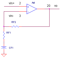
But, here's a big point regarding Aol and Acl
| The closed loop gain, Acl = RF2/RF1 + 1, is only valid when the open-loop gain Aol is much larger than Acl. That's why designers lose much blood, sweat and tears getting Aol as big as they can. The benefits are huge - more accurate closed-loop gain, lower distortion and lower output impedance. |
AMPLIFIER DESIGN
Let's step through a simple audio amp with a signal gain of 10 V/V (20 dB). We'll run it from a +/- 15V supply.
► Example Audio Amplifier
► DC BIAS
First, what is the bias current of Q1 and Q2? The current through RE splits into Q1 and Q2, so we calculate
Ic1 = Ic2 = 1/2 (VCC - VbeQ1) / RE = 1/2 (15 - 0.7) / 14.3k = 0.5 mA
Initially set RC1 to 0.7V/0.5mA = 1.4k to get Ic1 = 0.5 mA. But RC1 needs some tweaking until Ic1 = Ic2 approximately. (We'll do that later in the simulation to get RC1=1.8k).
Q3's collector current is calculated as
Ic3 = (VCC - VbeQ4) / RC3 = (15 - 0.7) / 4k = 3.6 mA
► AC SMALL-SIGNAL GAIN
The transconductance of Q1
gm1 = Ic / VT = 0.5 mA / 26mV = 0.0192 (A/V)
The current output of the differential input stage is
ic1 = vin · 1/2 · gm1 = vin · 1/2 · 0.0192 = vin · 0.0096 (A/V)
With beta3 = 100, Q3's input resistance becomes
rin3 = β / (Ic3 / VT) = 100 / (3.6 mA / 26 mV) = 727Ω
Collector current ic1 will split between RC1 and rin3, defined by
Ki = ib3 / ic1 = RC1 / (RC1 + rin3) = 1.8k / (1.8k+727) = 0.712
Q3 converts Q1's output to voltage by beta3 * RC3. The overall open-loop gain becomes
Aol = vc3 / vin = 1/2 gm1 · Ki · beta3 · RC3 = 2739 (V/V)
Finally, with Aol so large, we can confidently close the loop with RF1 and RF2 setting the closed-loop gain
Acl = vo / vin+ = RF1/RF2 + 1 = 100k/11k + 1 = 10 (V/V)
Excel Spreadsheet Here's a handy file that performs the above calculations: Basic_Amplifier_Calc.xls.
GAIN OF 10
Enough talk, let's do the walk. Run a Transient Analysis simulation of BASIC_AMPLIFIER.CIR. Voltage source VS generates a 0.1 V peak sine wave at 1 kHz. Plot the input V(1) and the output V(20). Does our predicted gain of 10 hold true? You should see an output of approximately 0.1V x 10 = 1.0 V. Cool beans! Our collection of parts actually functions as an amplifier.
CIRCUIT INSIGHT How well are Ic1 and Ic2 balanced? Open a new window and plot IC(Q1) and IC(Q2). Good news - they're both around 500 uA. Try adjusting RC1 up or down from 1800 to values like 1600 or 2000 ohms. Rerun the simulation to see it's effect on current balance. Then remove this added window. Now adjust the signal gain to values like 2 or 100 by scaling RF1 up or down. Does the signal gain change accordingly?
CLIPPING AND LOADING EFFECTS
Return the values to RF1 = 11k, RF2 = 100k, RL = 100k, CF1 = 10 uF and all transistor BF's to 100..
HANDS-ON DESIGN Run a Transient Analysis and plt the input V(1) and output V(20). Now, start increasing VS to 1 V and beyond. At what input level does the output start clipping? What is the clip level?
Try decreasing RL from 100k to 10k, 1k or 100 ohms. What happens to the clip level? Bad news. It occurs at a lower voltage level! How can you counter this loading effect and push it back up? Try increasing the beta of Q4 and Q5 from BF = 100 to 200 or 250. Does the clip level increase? Why? There's a limit of how much current the Q3 stage can supply to the bases of Q4 and Q5. More beta in Q4 means that for a given load current, there's less base drive required from the Q3 stage. This should allow Vo to swing higher, delivering more output current to RL.
MEASURING OPEN-LOOP GAIN
Let's switch over to AC Analysis to check out the open-loop gain. How do we measure this? We'll simply set the signal gain Acl to something far beyond the expected open-loop gain Aol. The resulting measured gain will reveal Aol.
CIRCUIT INSIGHT
Return the component values to RF2 = 100k, RL = 100k and all
transistor BF's to 100. Then set RF1 = 1 ohm and CF1 = 1000uF. This
theoretically sets Acl = 100,000 V/V far beyond our calculated Aol ~ 2700 V/V.
Run an AC Analysis with VS = 1 and plot Aol
as V(20)/V(1). Nice! The
open-loop gain reaches
about 2600 V/V. For a better view, change the y-axis to log scale. Check out
the transconductance of the differential stage by opening a new window and
plotting IC(Q1) / (V(2)-V(3)). Is it close to the value calculated above?
HANDS-ON DESIGN Suppose you wanted more open-loop gain in hopes of improving the distortion performance? Try increasing the Q1, Q2 bias by lowering RE. This increases the transconductance gm1 of the stage, increasing the overall gain. Lower RE to a value like 10k or 8k. What happens to Aol? You can also try Q3 with a larger beta. Increase BF for Q3 and check the Aol.
Finally, lower RL to values like 10k or 1k. What happened to the gain? Increasing the beta of Q4 and Q5 should restore some gain. Unfortunately, power transistors don't come with huge beta's. That's why you may need a Darlington pair in the output stage to get the beta you want when driving a low impedance loads.
COMPENSATION CAP CC
What is the role of this humble little capacitor sitting almost unnoticed at Q3? Let's find out its effect on the amplifier.
CIRCUIT INSIGHT Return the values to RF1 = 11k, RF2 = 100k, RL = 100k, CF1 = 10 uF and all transistor BF's to 100. Run an AC Analysis and plot the closed-loop gain V(20)/V(1). How high is the bandwidth? This response extends beyond 1MHz. Let's reel it in a bit by increasing CC by a factor of 10 or so. Keep decreasing CC until you're down below 100 kHz.
Why decease the bandwidth - isn't more better? In a feedback amplifier, decreasing the bandwidth is usually necessary to keep it from oscillating. (Because we're using ideal transistors in this simulation, this amplifier is pretty stable.) But in a later topic, we'll put in real world devices without CC and then watch it sing! Also, if its low noise you're after, then more bandwidth is a bad thing. Because, noise increases with increasing bandwidth, you'll only want to allow as much bandwidth as needed!
BUT WAIT - THERE'S MORE!
When you first start reading about audio amps (and op amp topologies), there are mountains of literature related to them. And it feels like you're mostly wandering in the dark valley trying to put it all together. But, that's what's satisfying - discovering over time using analysis, experimentation and simulation, how these fascinating circuits work.
Special thanks to John Ruiz for bread-boarding the amplifier above. Its fun to see that after all the calculations and simulations are done, the real deal actually works.
In this topic, we scratched the surface. The topics below look at enhancing performance by modifying each stage.
SPICE FILE
Download the file or copy this netlist into a text file with the *.cir extension.
BASIC_AMPLIFIER.CIR - DISCRETE AMPLIFIER
*
VS	1	0	AC 1	SIN(0 0.1V 1KHZ)
CIN	1	2	1UF
RIN1	2	0	100K
*
* POWER SUPPLIES
VCC	100	0	DC	+15V
VEE	101	0	DC	-15V
*
* DIFF AMP
RE	100	8	14.3K
Q1	4 2 	8	QPNP
Q2	101 3	8	QPNP
RC1	4	101	1800
*
* GAIN STAGE AND COMPENSATION
Q3	14 4	101	QNPN3
CC	14	4	10PF
*
* OUTPUT STAGE BIAS
RC3	100	11	4K
D1	11	13	D1N4148
D2	13	14	D1N4148
*
* OUTPUT STAGE
Q4	100 11	20	QNPN4
Q5	101 14	20	QPNP5
*
* LOAD
RL	20	0	100000
*
* FEEDBACK
RF2	20	3	100K
RF1	3	21	11K
CF1	21	0	10UF
*
* SMALL SIGNAL DEVICES
.model	QNPN	NPN(BF=100)
.model	QPNP	PNP(BF=100)
.model	QNPN3	NPN(BF=100)
.model	D1N4148	D(Is=0.1p Rs=16 CJO=2p Tt=12n Bv=100 Ibv=0.1p)

* OUTPUT POWER DEVICES
.model	QNPN4	NPN(BF=100)
.model	QPNP5	PNP(BF=100)

*
.TRAN	50US 2MS
.AC DEC 5 1 1MEG
.PROBE
.END
© 2007 eCircuit Center