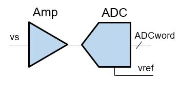
Basic Amplifer and ADC
Op Amp, 12-Bit ADC, +5V Ref
A basic amplfier and ADC provide great insight into a multi-stage Error Budget Analysis! We'll do a teardown of this critical and challenging analysis. You'll get
- a step-by-step approach
- walk thru each error source
- derive the circuit and sensitivity equations
- an Excel file
- enter errors in a systematic format
- vary parameters, see their effect on total error
- customize & expand template for your own designs
For Tutorials and more examples, see EBA Series
OFFSET AND GAIN ERRORS
What are the basic definitions of an amplifier's Offset and Gain Errors?
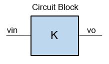
- Ideal Amplifier with Gain K
- Vo = Vin*K
- Actual Amplifier with errors
- Vo = Vin* (K+∆K) + ∆Voffset
- ∆K - Gain Error
- change in Gain from ideal (K).
- also called Slope, Span error
- ∆Voffset - Offset Error
- change in offset from ideal (0V)
- also called Intercept, Zero Error
- Combined Offset and Gain Errors
- Error = ±∆Voffset + ( ±∆K x Reading )
MAX ERROR BUDGET
The max budget (target spec) for amplifier has been chosen as:
- Offset Error: ∆Voffset = 5mV
- Gain Error: ∆K = 1% of Reading
AMPLIFIER AND ADC
Schematic with Errors
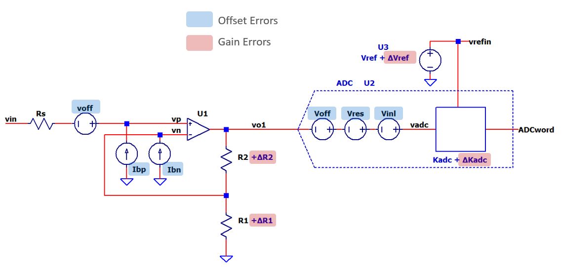
Three devices make up this signal-chain.
- U1, Op Amp
- U2, 12-bit ADC
- U3, +5V Reference
Device Errors
The errors below reflect a medium precision of accuracy grade for the devices.
Description Initial Temp Drift OFFSET ERRORS U1, voff, Input Offset Voltage
U1, ib, Input Bias Current
U1, iboff, Input Offset Current
U2, voff, Offset Error
U2, vres, Resolution Error
U2, vinl, Integral-Non Linearity Error1 mV
5 nA
5 nA
3 LSB
1/2 LSB
1 LSB10 uV / C
1 nA / C
1 nA / C
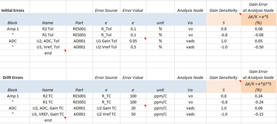
0.05 LSB/CGAIN ERRORS R2 Tolerance, Tempco
R1 Tolerance, Tempco
U2, Gain Tol, Tempco
U3, Vref Tol, Tempco0.1 %
0.1 %
2 LSB
0.5%100 ppm / C
100 ppm / C
0.08 LSB/C
50 ppm/C
Conditions and Assumptions
Temperature
- Ambient: Ta = 25C
- Max change: ∆T = 30C
Amplifier
- Rs = 500, R1=10k, R2=40k
- Vin = 1V, Vo = 5V
ADC
- Bits = 12
- Vref = 5.0V
Errors
- All errors can be either polarity +/-.
- Errors will be Referred to Input (RTI)
- Errors totalled as Worst Case (sum absolute values)
OFFSET ERRORS
While the steps below may seem more detailed than needed for simpler errors,
the value of creating a systematic approach can pay off when
analyzing more complex, multi-stage designs.
AMPLIFIER ERRORS
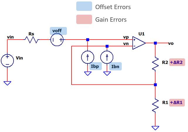
For errors (voff, ib, iboff, R1, R2, Aol), see Amplifer Advanced Analysis.
ADC OFFSET ERROR
The ADC's offset errors are typically characterized in units of digital output LSB's (Least Significant Bits). It's easy to convert output LSBs to input Volts using the ADC's resolution Vlsb.
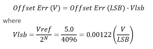
| Description | Initial Errors | Drift Errors |
| Error Source: e | offset = 3 LSBs Convert to V: voff = 3 LSB x x 0.00122 (V/LSB) = 3.66 mV |
offset_TC = 0.04 LSB/C Convert to V: voff_TC = 0.04 LSB /C x 0.00122 (V/LSB) = 49 uV / C |
| Pick Analysis Node: Va | vadc | vadc |
| Calc Sensitivity: S How does e impact Va? |
S = vadc / voff = 1 |
S = 1 |
| Calc Offset Error at Analysis Node Initial: ∆Voffset = e * S Drift: ∆Voffset = e * ∆T * S |
∆Voffset = 3.7 mV * 1 = 3.7 mV |
∆Voffset = 49uV/C * 30C * 1 = 1.5 mV |
| Calc Gain from Input to Analysis Node: Ka = Va / Vin |
Ka = vadc/vin = R2/R1+1 = 5 |
Ka = 5 |
| Calc Error RTI (Referred-to-Input): ∆voffset_RTI = ∆voffset / Ka |
∆voffset_RTI = 3.7 mV / 5 = 0.73 mV |
∆voffset_RTI = 1.5 mV / 5 = 0.3 mV |
ADC RES & INL ERRORS
The Resolution Errors and Integral Non-Linearity (INL) Errors are considered part of the offset errors. Why? Mainly because they don't scale directly with the signal level (which would imply a gain term).
- Resolution Error - also called Quantization error, creates an error of 1/2 LSB.
- INL Error - varies with signal level, but does not scale with the signal level.
The error analysis for both of these ADC errors follow the same steps as the Initial Offset Error shown above. (See Excel file link below.)
GAIN ERRORS
Similar to Offset Errors, the Gain Errors can be converted from LSBs to % or ppm.

ADC GAIN ERROR
You can write the ADC gain as
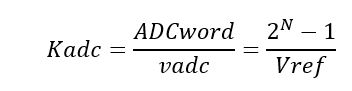
Because Kadc directly defines gain of this block, you can assume the Sensitivity is unity,
or S = 1.0.
| Description | Initial Errors | Drift Errors |
| Error Source: e | Kadc_Tol = 2 LSB Convert to %: Kadc_Tol = 2LSB/4095*100% = 0.05% |
Kadc_TC = 0.08LSB/C Convert to ppm/C: Kadc_TC = 0.08LSB/4095*1e6 = 20ppm/C |
| Pick Analysis Node: Va | ADCword | ADCword |
| Calc Sensitivity: S How does e impact Gain K? |
S = 1.0 (see discussion above) |
S = 1.0 |
| Calc Gain Error at Analysis Node Initial: ∆K/K = e * S Drift: ∆K/K = e * ∆T * S |
∆K/K = 0.05% * 1.0 = 0.05% |
∆K/K = 20ppm/C*30C*1.0 = 600ppm = 0.06% |
| Normailzed gain errors can be referred to input as-is, no RTI calc needed. |
VREF ERROR
The Vref term appears in the denominator of the ADC gain.
Intuition tells us the Sensitivity S should be negative (as
Vref goes up, Kadc goes down.) We can also guess that the magnitude of S should be 1
because Vref is a direct multiplier (numerator or denominator) of the gain.
We'll calculate S anyway below just to confirm.
| Description | Initial Errors | Drift Errors |
| Error Source: e | Vref_Tol = 0.5% |
Vref_TC = 50 ppm/C |
| Pick Analysis Node: Va | ADCword | ADCword |
| Calc Sensitivity: S How does e impact Gain K? Apply Difference Method: S = (∆K/K)/(∆V/V) where ∆K = (K'-K) |
Kadc = ADCword/vadc = (2N-1)/Vref Vref = 5.0 2N-1 = 4095 Kadc = 4095/5 = 819 Kadc' = 4095/(5*1.01) = 811 ∆Vref/Vref = 0.01 S = (∆Kadc/Kadc) / (∆Vref/Vref) = -1.0 |
S = -1.0 |
| Calc Gain Error at Analysis Node Initial: ∆K/K = e * S Drift: ∆K/K = e * ∆T * S |
∆K/K = 0.5% * -1.0 = -0.5% |
∆K/K = 50ppm/C*30C*-1.0 = -1500ppm = -0.15% |
| Normailzed gain errors can be referred to input as-is, no RTI calc needed. |
SUMMARY & EXCEL FILE
See Excel file: amp-ref-ADC-1-EBA.xlsx
Right Click on the filename, select "Save link as...".
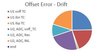
OFFSET ERRORS
Calculate the total using Worst Case Analysis. WCA assumes the most unfavorable conditions: all errors at their maximum limit AND in the same polarity.
- WCA = | ∆Voffset1 | + | ∆Voffset2 | + ...
= 2.2mV
Does the Total Error fly under the Max Error Budget (Requirements)?
- WCA < 5.0mV?
Yes - PASS!
GAIN ERRORS
Calculate the total using Worst Case Analysis.
- WCA = | ∆K1 | + | ∆K2 | + ...
= 1.4 %
Does the Total Error fly under the Max Error Budget (Requirements)?
- WCA < 1.0%?
No - FAIL!
Yikes! Can we improve the design? See "Try It" below.
EBA WITH EXCEL
An Excel file was created to implement the error budget analysis.
- Organizes complex analyses into smaller managable sections
- Easier to create, review and debug
- Customizable and expandable to more complex circuits
- Modular for reuse in other designs
3 Worksheets
Worksheet Enter Calculate CIRCUIT CALC Circuit values Signal gains / levels and Sensitivities (S) OFFSET Offset error sources Offset errors and totals GAIN Gain error sources Gain errors and totals
While 3 worksheets may seem over-the-top for smaller circuits, you'll find a big advantage when analyzing more complex circuits or multi-stage systems!
Try the hands-on spreadsheet!
- Excel file: amp-ref-ADC-1-EBA.xlsx
Right Click on the filename, select "Save link as...". - Open file, explore the Calc, Offset and Gain Sheets
- Play in the sandbox, modify values, see the impact on errors.
- Copy to a new file - experiment!
TRY IT!
- The Total Gain Error did NOT meet spec! Can we improve the design?
- Open the Excel file. Check the Gain Error Sheet to identify the largest error contributors.
- Try changing the R1 and R2 tempcos from 100 ppm/C to a higher precision - a 50, 25 or 10 ppm/C tempco.
- Try changing the +5V Ref tolerance from 0.5% to 0.1%.
For in-depth tutorials and more circuits, go to
EBA Series