Guitar Effect - Phase Shifter
CIRCUIT
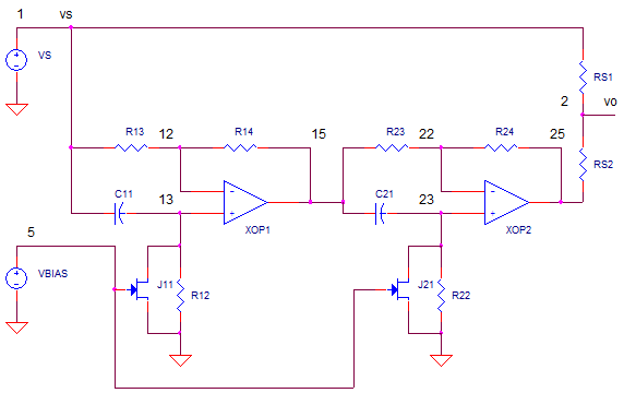
OP_PHASE_SHIFTER_JFET1.CR Download the SPICE file
The phase shifter creates a pleasing swirling sound found on many
recordings. The opening guitar solo on Eddie Van Halen's
"Eruption" combines a phase shifter with a distortion box.
How do they create that sound? Further confounding was the initial
literature I read describing a notch filter where the notch frequency is
swept back and forth across the spectrum at a slow rate. Sounded
impossible to fit all that circuitry into a small effect pedal. Turns
out the notches were created using a clever, but straightforward method.
NOTCH FILTER
The notch filter is fairly straight forward to construct. Essentially
you split the audio signal into two paths - one as-is and the other
delayed. Then add the signals back together. For signals whose delayed
path is an inverted version of the original, the sum becomes zero!
TIME DELAY
How do you create a time-delay? The
all-pass filter is a perfect candidate - it passes all signals with
unity gain, while changing their delay (phase) over a specific frequency
range. At a single frequency fc, the phase shift is -90 deg. Taking it a
step further, cascading two stages provides a total of -90 + -90 = -180 deg
shift at a single frequency fc!
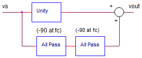
Of course, a phase of -180 deg (half-wave time delay) is also interpreted as an
inverted version of the original. Summing the original and the -180
deg delayed signal together and you've got 0 signal output! Or
putting it another way, you've got a deep notch at fc.
CHEAP SUMMER
The summing function
is simply two resistors, RS1 and RS2, that essentially take the average of
the two signals V(1) and V(25).
V(2) = (V(1) + V(25)) / 2
NOTCH SWEEPER
What gives the phase shifter effect pedal it's swirling sound? The
"swirl" is actually the sweeping of notch frequency back and forth at a slow
rate. How is this accomplished? Because the notch is determined by R11 and
C11, a variable resistor (JFET) is placed across R12. Many applications call
on the JFET to act as
a variable resistor where the drain-source resistance Rds decreases with
increasing gate voltage.
The final piece of this puzzle requires a slow moving triangle wave
applied to the JFET's gate to vary the resistance, and thus fc, at a slow
rate. The triangle wave is typically easily created with a op amp based
oscillator.
FREQUENCY RESPONSE
With R1=10k and C1=0.1uF, we expect to find a notch at fc = 1/(2·pi·10k·0.1uF)
= 159 Hz.
CIRCUIT INSIGHT
Run an AC ANALYSIS of OP_PHASE_SHIFTER_JFET1.CIR and plot the input
V(1) and output V(2). I remember the first SPICE run of this circuit and
being pleasantly surprised at the deep notch at around 160 Hz. Also, I
wanted to see the phase shift at the all-pass output path hitting -180 deg
(inverted signal) at fc. Add a plot pane and add trace V(25). What is the
phase at 160Hz?
TRANSIENT RESPONSE
Now let's watch a sine wave travel down the normal and delayed path. Voltage
source VS creates a 100 mV sine wave to help us see the time delay. SPICE lets you
set the sine wave frequency using the .PARAM command. For example, set fo to
a low frequency like 1.6Hz simply use
.PARAM fo=1.6Hz
The variable fo also sets the length of simulation time
.TRAN 0.1MS {4/fo}
to conveniently include several sine cycles. For now we leave the JFETs biased OFF with -2.3V at their gates.
NO DELAY Run a TRANSIENT ANALYSIS and plot the input V(1) and the delayed path V(25). What is the expected output? Because the sine wave at 1.6 Hz is well below fc=160 Hz, the sine wave should NOT be delayed by much through the all-pass path. In fact, V(25) should look almost identical to V(1). Finally taking the average gets you the original magnitude of 100mV back.
SMALL DELAY Rerun the simulation with fo=16 Hz. Does the time delay through the filter progressively shift as the frequency increases? Cool beans - we start to see a small time delay (phase shift), yet the magnitude stays the same! However, the delay is still too small for the sum at V(2) to change magnitude.
-180 DELAY Now for the big moment. Rerun the simulation with fo=160 Hz. How much delay has occurred? Yes, the time shift is one half cycle (-180 deg) making it appear inverted. What happened at the summer output? As intended, the average of a +1 and -1 magnitude is ZERO! Mission accomplished; the filter creates a notch at 160 Hz.
JFET NOTCH SWEEPER
The final question: Lastly, how can we sweep the notch back and
forth? Many phase shifters use a
JFET (Variable
Resistance) in parallel with the delay setting components R12 and R22.
AC ANALYSIS Run an AC ANALYSIS and plot the input V(1) and output V(2). Like before, you should see a notch at fc=160 Hz. Now try adjusting VBIAS from --2.3V to -2.2V and so on.
VBIAS 5 0 DC -2.3V
Each time rerunning the simulation to see when and how far the notch moves. Will the notch move higher or lower in frequency? Because, the JFET's parallel resistance will essentially lower the resistance across R12, we expect the notch to move up in frequency.
TRANSIENT ANALYSIS Finally, if you want to see the sweeper in action in the time domain, set the sine wave to fo=400 Hz. Also, let's drive the JFET gates with a triangle wave created byu the PULSe command. Simply uncomment these commands and place a "*" in front of the existing VBIAS and TRAN commands.
.PARAM Trate=1s
VBIAS 5 0 PULSE(-2.1V -1.75V 0MS {Trate*0.49} {Trate*0.49}
.TRAN 1MS 1000MS
By defining very long rise and fall times, a triangle is created. Here's the PULSE command and its parameters.
.PULSE( {v1} {v2} {tdelay} {trise} {tfall} {width} {period} )
Run a TRANSIENT ANALYSIS and plot the ramp V(5) and output V(2). At what ramp voltage (JFET gate) does the notch frequency hit 400 Hz and attenuate the signal?
SPICE FILE
Download the file or copy this netlist into a text file with the *.cir extension.
* op_phase_shifter_JFET1.cir
*
.PARAM fo=1.6Hz
VS 1 0 AC 1 SIN(0V 0.1V {fo})
* GATE VOLTAGE
.PARAM Trate=1s
*VBIAS 5 0 PULSE(-2.1V -1.75V 0MS {Trate*0.49} {Trate*0.49} {Trate*0.01} {Trate} )
VBIAS 5 0 DC -2.3V
*
C11 1 13 0.1UF
R12 13 0 10k
J11 13 5 0 J2N5952
R13 1 12 10K
R14 12 15 10K
XOP1 13 12 15 OPAMP1
*
C21 15 23 0.1UF
R22 23 0 10k
J21 23 5 0 J2N5952
R23 15 22 10K
R24 22 25 10K
XOP2 23 22 25 OPAMP1

* summer
RS1 1 2 10k
RS2 25 2 10k
*
*
.model J2N5952 NJF(Beta=1.314m Betatce=-.5 Rd=1 Rs=1 Lambda=4m Vto=-2.021
+ Vtotc=-2.5m Is=33.57f Isr=322.4f N=1 Nr=2 Xti=3 Alpha=311.7u
+ Vk=243.6 Cgd=1.6p M=.3622 Pb=1 Fc=.5 Cgs=2.414p Kf=10.14E-18 Af=1)
*
* OPAMP MACRO MODEL, SINGLE-POLE
* connections: non-inverting input
* | inverting input
* | | output
* | | |
.SUBCKT OPAMP1 1 2 6
* INPUT IMPEDANCE
RIN 1 2 10MEG
* GAIN BW PRODUCT = 10MHZ
* DC GAIN (1MEG) AND POLE 1 (10HZ)
EGAIN 3 0 1 2 1000K
RP1 3 4 1K
CP1 4 0 15.9UF
* OUTPUT BUFFER AND RESISTANCE
EBUFFER 5 0 4 0 1
ROUT 5 6 10
.ENDS
*
* ANALYSIS *************************************
*.TRAN 0.1MS {10/fo}
*.TRAN 1MS 1000MS
.ac dec 100 1 100k
.PROBE
.END
© 2012 eCircuit Center