JFET Variable Resistor
CIRCUIT
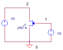
JFET_VARIABLE_RES1.CR Download the SPICE file
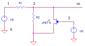
JFET_VARIABLE_ATTEN1.CR Download the SPICE file
Some designs call for a
variable resistor such as variable gain amplifiers,
attenuators and some guitar effect boxes. The main goal here is
applying a device whose resistance is some function of bias
voltage. One such device is your basic JFET. For small
signals, where the device operates in the linear (or ohmic) region, the resistance between
the Drain and Source terminals (Rds) decreases as the
gate voltage increases.
IV CURVES
How can you determine the JFET resistance versus
bias voltage? Nothing tells the story like the slope of
the IV curve. Here's the basic circuit to develop these
insightful graphs.
* GATE AND DRAIN VOLTAGE
VG 1 0 DC 0
VD 2 0 DC 0
J1 2 1 0 J2N5952
*
* Nested DC sweep
.DC VD -0.05 0.05 0.1 VG -1.75 0 0.25
The file includes an essential line - the nested DC sweep command.
.DC V1 Start Stop Incr V2 Start Stop Incr
You define how the test voltages V1 and V2 will start,
stop and increment. Then, for each V1 voltage point, V2
will sweep through its entire range from start to stop.
This comes in handy where the drain (VD) is swept through
its range for every gate bias voltage (VG).
CIRCUIT INSIGHT Run a DC analysis of the 2N5952 JFET in the file JFET_VARIABLE_RES1.CIR and plot the drain current ID(J1). The drain is swept through a narrow range -50mV to +50mV. You should see a nice family of curves representing Id as a function of Vd for each value of Vg.
The slope of each VI curve represents the Drain-Source resistance.
- The highest resistance (smallest slope) can be approximated by Rds = 50mV/38uA = 1.33k ohms.
- The lowest resistance (highest slope) is Rds = 50mV/250uA = 200 ohms.
This shows the range of resistance possible when sweeping the gate from -1.75 to 0V. Try plotting the resistance by adding a plot window and adding trace V(2)/I(VD).
As warned earlier, this resistor-like operation
applies only to small signals. What about larger signals?
Increase the Vd sweep parameters to Start = -0.5V and
Stop = +0.5V. What happens to the linearity of the IV
plots?
VARIABLE ATTENUATOR
Here's an application of a JFET taken straight out
of a National App note. The JFET implements a
voltage attenuator as one leg in a voltage divider.
The voltage divider ratio is defined by Vo/Vs = R2'/(R1+R2') where R2' is actually the parallel combo of R2 and Rds. For this example, setting R1=10k and R2=100k defines a small attenuation, even when the JFET is OFF (very high resistance)
CIRCUIT
INSIGHT The gate voltage VG ramps from -2V
to 0V while a 100mV (1kHz) sine wave is applied to the
divider input. Run a TRANSIENT ANALYSISs of
JFET_VARIABLE_ATTEN1.CIR and plot both the gate voltage
(V3) and the output voltage V(2). At what gate voltage
does Rds begin conducting and attenuating the signal?
Where does the max attenuation occur? You can estimate
Rds by measuring V(2) peaks and solving the divider
equation for R2.
UPCOMING TOPICS
In a future topic, we'll use the variable resistor
as part of a popular guitar effects pedal called the
phase shifter.
SPICE FILES
Variable Resistor
Download the file or copy this netlist into a text file with the *.cir extension.
* JFET_VARIABLE_RES1.CIR
*
* GATE AND DRAIN VOLTAGE
VG  1 0       DC 0
VD  2 0       DC 0
*
J1  2 1 0 J2N5952
*
* Nested DC sweep
.DC  VD -0.05 0.05 0.1   VG -1.75 0 0.25
*
*
.model J2N5952	NJF(Beta=1.314m Betatce=-.5 Rd=1 Rs=1 Lambda=4m Vto=-2.021
+ Vtotc=-2.5m Is=33.57f Isr=322.4f N=1 Nr=2 Xti=3 Alpha=311.7u
+ Vk=243.6 Cgd=1.6p M=.3622 Pb=1 Fc=.5 Cgs=2.414p Kf=10.14E-18 Af=1)
*
.PROBE
.END
Download the file or copy this netlist into a text file with the *.cir extension.
Variable Attenuator
* JFET_Variable_Atten1.CIR
*
VS	1	0	SIN(0 0.1V 1000Hz)
R1	1	2	10k
R2	2	0	100k
*
J1	2	3	0	J2N5952
VG	3	0	PWL(0ms -2.5V   100ms 0V)
*
.model J2N5952	NJF(Beta=1.314m Betatce=-.5 Rd=1 Rs=1 Lambda=4m Vto=-2.021
+ Vtotc=-2.5m Is=33.57f Isr=322.4f N=1 Nr=2 Xti=3 Alpha=311.7u
+ Vk=243.6 Cgd=1.6p M=.3622 Pb=1 Fc=.5 Cgs=2.414p Kf=10.14E-18 Af=1)
*
* ANALYSIS *************************************
.TRAN 	0.1MS  100MS
.PROBE
.END
© 2012 - 2026 eCircuit Center