ADC - Dual Slope Integrator
CIRCUIT
DUAL_SLOPE_CONVERTER1.CIR Download the SPICE file
A fascinating question has always been - how can you convert an analog voltage to an equivalent digital word? One of the many interesting architectures available is the dual-slope integrator. This clever Analog-to-Digital Converter (ADC) has been at the heart of the Digital Volt Meter (DVM) for decades. You can think of this method as a stop watch of sorts. Simply count the time it takes for the integrator voltage to ramp back down to zero volts. The time on the dial is proportional to the input voltage! Just a few basic components constructs this basic ADC implementation.
INTEGRATOR AND SWITCHES
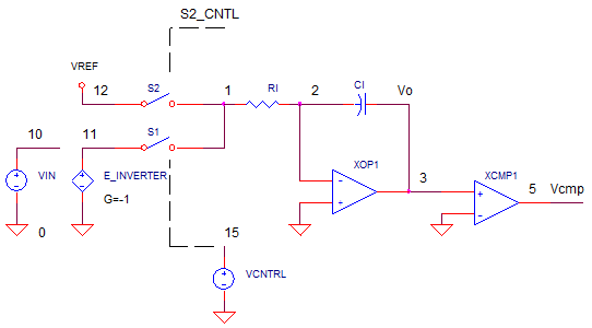
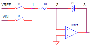
The basic DNA of this converter is your basic op amp integrator, two switches and a reference.
The name Dual Slope comes from its basic behavior of creating a waveform with a positive slope, followed by a negative slope. The entire conversion occurs in three phases.
1. RAMP UP - Integrate a Variable Input (Vin) for a Fixed Time (T1)
2. RAMP DOWN - Integrate a Fixed voltage (Vref) for a Variable Time (T2) until output returns to 0V.
Where is the conversion? The time interval T2 is proportional to the input voltage! Simply measure T2 with a oscillator and a counter. At the end-of-conversion, the DVM's display is updated with the new count value.
3. RESET - Short C1 for Vo = 0V
RAMP UP AND DOWN
The power of the Dual Integrator lies in independence on the Capacitor accuracy or drift! How is this possible? The simple mathematics of the circuit tells the story.
During the RAMP UP phase (starting at Vo=0V), the output increases with a variable slope (depending on Vin) for a fixed period T1. (See Integrator for a review)
V1 = -Vin / R1 · T1 / C1 RAMP UP ▲
(Notice, because the integrator is inverting, you need to invertVin for a positive slope.)
During the RAMP DOWN Phase, the output decreases to 0V at a Fixed Slope for a variable time T2. How far does Vo ramp down? The same voltage change as during ramp up.
V2 = -Vref / ( R1· C1) ·T2 RAMP DOWN ▼
Because the output ramps up and down equally (V1=V2) , you can write
Vin / ( R1· C1) ·T1 = Vref / ( R1· C1) ·T2
Note that the RC terms drop out and you are left with ratios Vin / Vref = T2 / T1. Solving for T2 you get
T2 = Vin / Vref · T1
This awesome result tells us that the the interval T2 varies in direct proportion to the ratio of Vin/Vref. So how can you get a digital word out of this? Simply let a coulter run during T2 and display it's result.
BIG DEAL! The cool thing about dual-slope converters is that the RC terms
drop out of the conversion result!
Typically, the accuracy of an integrator circuit largely depends the accuracy of R1 and C1. For example, a 1% error in C1 causes a 1% error at the output. But, as we discovered above, a converter with both a positive and negative slope places the accuracy on the ratio of slopes and intervals; not the exact slopes. The only precision component required is the reference VREF.
What about the accuracy of the clock driving the counter? Turns out that a faster or slower clock will not directly effect accuracy either! Just check that the slowest clock (a longer T1) will not cause the integrator to hit the rail during ramp up!
EXAMPLE CONVERTER
Let's design a +/-10V dual-slope converter with T1=T2=10ms. Choosing C1=0.1uF, calculate R1 for a max Vo=10V for Vin=10V during T1=10ms.
.R1= -Vin / Vo · T1 / C1 = 100k
The total convert time will be at least T1+T2=20ms plus the Reset Phase T3.
SPICE MODEL
VIN and VREF define the input and reference voltages respectively. To get a positive slope during T1, we'll invert VIN using controlled source E_INVERTER with gain set to -1. Analog switches S1 and S2 (defined by models SWA and SWB) are controlled by VCNTL. This switch control signal turns S1 ON (S2 OFF) during T1 and then turns T2 ON (T1 OFF) during T2.
Components R1, C1 and XOP1 create a classic op amp integrator. The Reset Phase simply returns C1s voltage to 0V. To keep things simple, we'll avoid the reset circuitry and use the Initial Condition option (IC=0V) to set the initial cap voltage.
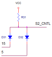
Comparator XCMP1 indicates when the integrator output V(3) crosses 0V. This zero-crossing provides us the measurement of T2, and ultimately the measure of VIN!. Also, we'll stop the integrating at the end of T2 by opening S2. This is accomplished by ANDing the VCNTL and XCMP1 outputs using a diode-based AND gate (see R31, D31 and D32.).
The comparator's model is created in a subcircuit COMP1. A simple piece-wise-linear table describes XCMP's input / output relationship.
EOUT 5 0 TABLE {V(4)} = (-0.5MV 0V) (0.5MV, 5V)
This behavioral model defines three cases
(Vin+-Vin-) > +0.5mV Vo = 5V
(Vin+-Vin-) < -0.5mV Vo = 0V
-0.5mV < (Vin+-Vin-) < +0.5mV. G = ( 5V - 0V ) / (+0.5mV - (-0.5mV) ) = 5000.
CONVERTER TEST
To test our converter, we'll apply an input of VIN=9.5V. Run a TRANSIENT SIMULATION of the file named DUAL_SLOPE_CONVERTER1.CIR.
CIRCUIT INSIGHT Plot the switch control VCNTL at V(15) and the comparator output at V(5). In another pane, plot the integrator output at V(3). What is the converter output? Find when the comparator output falls (T_fall) indicating the end of the ramp down interval and calculate
T2 = T_fall - T1.
As an example, for T_fall=19.0599 ms, calculate T2 = 19.5099 ms - 10ms = 9.055ms. Finally, determine the VIN as
VIN = T2 / T1 * Vref
= 9.5099ms / 10ms * 10V
= 9.5099 V
The converter has delivered as promised! The reading of VIN lands within 0.1% of Full Scale.
ACCURACY AND NOISE
Suppose you specified a capacitor with 5% tolerance. Let's check its effect on accuracy when you get a worst case value. Change C1 to 0.105uF and rerun the simulation. What impact did the 5% change have on T2? The comparator output falls at essentially the same time as for the ideal C1=0.1uF. Why? The RC terms have dropped out of the conversion calculation. This highlights one compelling reason that the dual-slope converter has become the work horse of the Digital Volt Meter (DVM).
CIRCUIT INSIGHT What about the converter's accuracy in the presence of noise? Inject some noise via VN defined as a sine wave. Change its peak value from 0V to 0.5V.
VN 20 0 SIN(0Voff 0.5Vpeak 3kHz)
NOTE: This big ugly noise source tramples on top of the VIN! (Using a different style converter that captures the instantaneous signal value, this noise would be devastating to the accuracy.) However, the integrator's inherent low-pass behavior puts the kabash on higher frequency noise. Rerun the simulation and check when V(5) falls. What is the impact of the 5% peak error signal on T2?
DMM SERIES
Measure DC Volts with a Decade
Resistor Resistor Network.
Measure DC Current with a Decade
Current Sense Resistor Network.
Discover the heart of most DMM's - the
Dual-Slope Integrator.
SPICE FILE
Download the file or copy this netlist into a text file with the *.cir extension.
DUAL_SLOPE_CONVERTER.CIR
*
* INPUT VOLTAGE
VIN	10	20	9.5VDC
VN	20	0	SIN(0Voff 0Vpeak 3kHz)
*
* INVERT INPUT
E_INVERTER 11 0	10 0	-1
*
* REFERENCE VOLTAGE
VREF	12	0	10.0VDC
*
* CONTROL: VCNTRL=0 S1=ON, S2=OFF
*          VCNTRL=1 S1=Off,S2=ON
VCNTL	15	0	PWL(0MS 0V  10MS 0V 10.01MS 5V)
*
* INTEGRATOR
S1	11 1  15 0 SWB
S2	12 1  31 0 SWA
R1	1	2	100K
C1	2	3	0.10UF IC=0V
XOP1	0 2 3	OPAMP1
*
* COMPARATOR (ZERO CROSSING DETECTOR)
XCMP1	3 0 5 COMP1
*
* AND GATE, IF VCNTRL AND XCMP1 OUTPUTS ARE HI, THEN S2 = ON
VCC	30	0	DC	5V
R31	30	31	10k
D31 31	15	D1N4148
D32 31	5	D1N4148
*
*
* SUBCIRCUITS AND MODELS ***********************************
*
.SUBCKT COMP1  1 2 5
* TERMINALS: 1-INPUT+, 2-INPUT-, 5-OUTPUT
* DIFF AMP
EDIFF	3	0	VALUE = { V(1) - V(2) }
* FREQUENCY RESPONSE
RP1	3	4	500
CP1	4	0	1000PF
* LIMITER
EOUT	5	0	TABLE {V(4)} = (-0.5MV 0V) (0.5MV, 5V)
.ENDS
*
*
* OPAMP MACRO MODEL, SINGLE-POLE WITH 15V OUTPUT CLAMP
* connections:      non-inverting input
*                   |   inverting input
*                   |   |   output
*                   |   |   |
.SUBCKT OPAMP1	    1   2   6
* INPUT IMPEDANCE
RIN	1	2	10MEG
* DC GAIN=100K AND POLE1=100HZ
* UNITY GAIN = DCGAIN X POLE1 = 10MHZ
EGAIN	3 0	1 2	100K
RP1	3	4	100K
CP1	4	0	0.0159UF
* OUTPUT BUFFER AND RESISTANCE
EBUFFER	5 0	4 0	1
ROUT	5	6	10
.ENDS
*
.MODEL	SWA	VSWITCH(VON=5 VOFF=0 RON=1 ROFF=1e12)
.MODEL	SWB	VSWITCH(VON=0 VOFF=5 RON=1 ROFF=1e12)
*
* DIODE
.model	D1N4148	D(Is=0.1p Rs=16 CJO=2p Tt=12n Bv=100 Ibv=0.1p)
*
* ANALYSIS *************************************************
.TRAN 	25US  20MS UIC
.PROBE
.END
© 2012 eCircuit Center