Source Measure Unit
Compliance Limits (Clamps)
How can an SMU limit the Voltage or Current?
Download SPICE Netlist or LTSPICE
Schematic
Right Click on filename, select "Save link as..."
How does the hardware protect against damage to the Device-Under-Test
(DUT) and the Source Measure Unit (SMU) itself? Two extreme conditions
are forcing voltage into a SHORT or forcing current into an OPEN. The compliance circuit
provides two limiting or clamping actions
- When Forcing Voltage, Clamp the Current.
- When Forcing Current, Clamp the Voltage.
You can set these Compliance Limits based on a maximum operating limits of the device or the SMU.
But how can we add these limits to the basic SMU circuit? By simply adding two error amplifiers to the servo loop, we can achieve clamping action. The final challenge is creating a Crossover circuit that seamlessly transfers control from Force Mode to Clamp Mode. (See Crossover Circuit topic.)
Get a refresh of the SMU Circuit
Back to the SMU Series
OVERVIEW
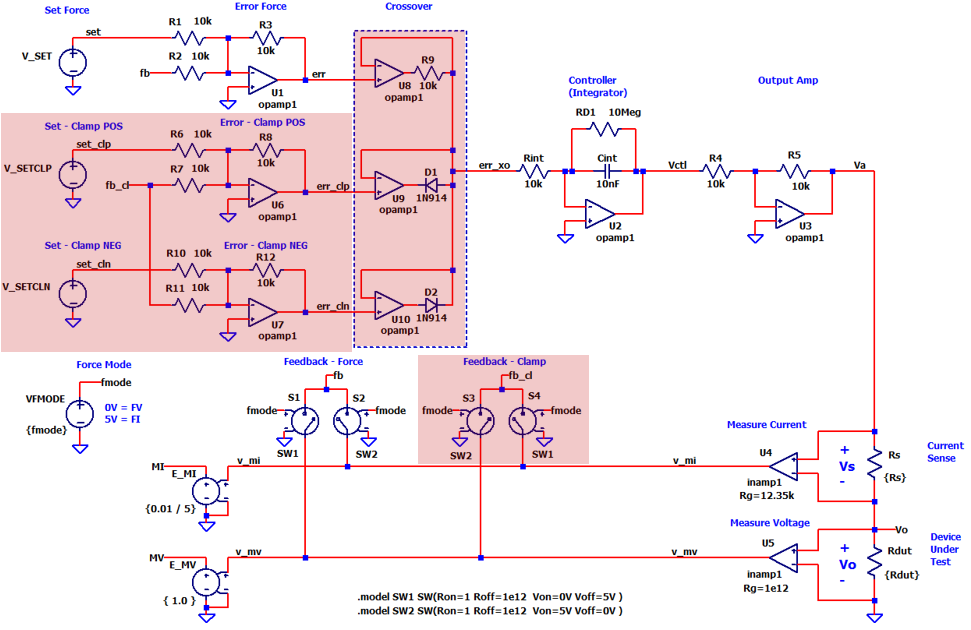
To expand our SMU's capacity to implement clamps, we add blocks (shaded in ORG) for the POS and NEG Clamps.
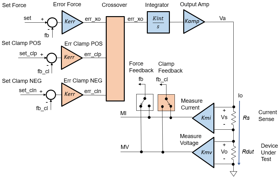
- Each of the three control modes - Force, POS Clamp and NEG Clamp - requires its own Error Amplifier.
- The Crossover Circuit pass through the MINIMUM of the three errors.
- The Clamp Feedback selects the opposite signal of the Force Feedback.
FORCE VOLTAGE, CLAMP CURRENT
As an example, suppose you want to force +5V with clamps set at +1mA and -1mA.
Set Points
- set = +5V
- set_clp = +1mA
- set_cln = -1mA
Feedback
- fb = MV (voltage)
- fb_cl = MI (current)
FORCE CURRENT, CLAMP VOLTAGE
Alternatively, suppose you want to force 1mA with clamps set at +5V and -5V.
Set Points
- set = 1mA
- set_clp = +5V
- set_cln = -5V
Feedback
- fb = MI (current)
- fb_cl = MI (voltage)
CLAMP CIRCUIT
The Error Amps for Clamps (U6, U7) look similar to one for Force (U1).
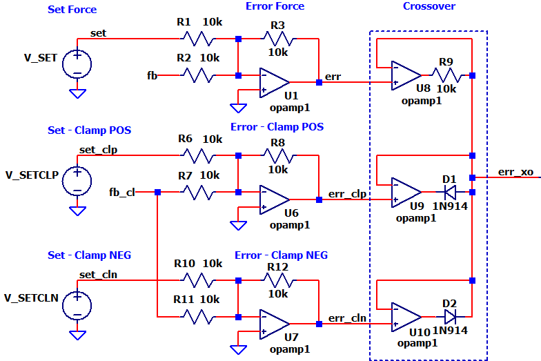
- The set points for POS and NEG CLAMP (typically DACs) are set by V_SETCLP and VSETCLN.
- The Clamp Feedback fb_cl is fed to both POS and NEG error amps.
- Error signals err_clp and err_cln measure the error between the clamp feedback and the set points.
- The Crossover is a clever circuit that passes through the MINIMUM of
the three errors: err, err_clp and err_cln.
(See Crossover Circuit topic!)
Feedback selected by switches S1 - S4 controlled by fmode (0V=FV, 5V=FI).
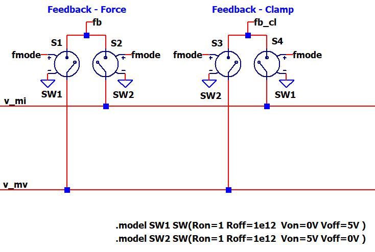
- Force VOLTAGE, Clamp CURRENT
- S1 ON: fb = MV
- S4 ON: fb_cl = MI
- Force CURRENT, Clamp VOLTAGE
- S2 ON: fb = MI
- S3 ON: fb_cl = MV
SMU SPECS
Here's a quick overview of the operating ranges of the SMU circuit:
- Vrange = +/-5V,
- Irange = +/-10mA
- Current Sense
- Rs = 100
- Vs = +/-1V Max
- Internal voltage range for feedback loop.
- Vset = +/-5V (5V or 10mA Range)
SIMULATION
Enable the relevant PARAM before running each test.
- SPICE Netlist: Remove the "*" before the PARAM statement. All others add "*" at beginning of statement.
- LTSPICE Schematic: Right-click the statement and select DIRECTIVE. All others select COMMENT.
FORCE V, CLAMP I Set the Force Voltage parameters (.param fmode=0V...) as a SPICE Directive. Set Force Current (.param fmode=5V...) as a Comment.
.param fmode=0V set=1V set_cl=1mA/10mA*5V Rs=100 Rdut=1000
- Force Voltage: 1V
- Clamp Current: 1mA on the 10mA Scale
- Sense Resistor: 100 ohms
- Device-Under-Test: Rdut = 2000
- Output Current: Idut = 1V / 2000 = 0.5mA
Run a Transient Simulation of SMU-circuit-clamps-1.cir (or *.asc). Add traces for output voltage v(vo) and current I(Rdut). Add another Plot Window and Add trace I(Rdut). Does Idut reach it's expected value of 0.5mA?
Now reduce Rdut to 500 ohms for an expected output current of 2mA. Rerun the Transient Simulation. Did the POS Clamp swing into action and limit the output current to 1mA?
FORCE I, CLAMP V Set the Force Current parameters (.param fmode=5V...) as a SPICE Directive. Set Force Voltage (.param fmode=0V...) as a Comment.
.param fmode=5V set=1mA/10mA*5V set_cl=2V Rs=100 Rdut=1000
- Force Current: 1mA on the 10mA Scale
- Clamp Current: 5V
- Sense Resistor: 100 ohms
- Device-Under-Test: Rdut = 1k
- Output Voltage: Vdut = 1mA * 1k = 1V
Run a Transient Simulation of SMU-circuit-clamps-1.cir (or *.asc). Add traces for output voltage v(vo) and current I(Rdut). Add another Plot Window and Add trace I(Rdut). Does Idut reach it's expected value of 1mA?
Now increase Rdut to 3k ohms for an expected output voltage of 3V. Rerun the Transient Simulation. Did the POS Clamp swing into action and limit the output voltage to 2V?
SPICE NETLIST
Download SPICE Netlist or LTSPICE
Schematic
Right Click on filename, select "Save link as..."
* SMU Circuit with Clamps
*
* Parameters
* FV Mode
.param fmode=0V set=1V set_cl=1mA/10mA*5V Rs=100  Rdut=1000
* FI Mode
*.param fmode=5V set=1mA/10mA*5V set_cl=2V Rs=100  Rdut=1000
*
* Set - Force
V_SET vset 0 PWL(0us 0 1us {-set})
*
* Error - Force
R1 vset  N002  10k
R2 N002  fb   10k
R3 err N002  10k
XU1 N002 0 err opamp1
*
* Set - Clamp POS
V_SETCLP set_clp 0 PWL(0us 0 0.1us {-set_cl})
*
* Error - Clamp POS
R6 set_clp N004 10k
R7 fb_cl N004 10k
R8 err_clp N004 10k
XU6 N004 0 err_clp opamp1
*
* Set - Clamp NEG
V_SETCLN set_cln 0 PWL(0us 0 0.1us {set_cl})
*
* Error - Clamp NEG
R10 set_cln N007 10k
R11 fb_cl N007 10k
R12 err_cln N007 10k
XU7 N007 0 err_cln opamp1
*
* Crossover
XU8 err_xo err N006 opamp1
R9 err_xo N006 10k
XU9 err_xo err_clp N005 opamp1
D1 err_xo N005 1N914
XU10 err_xo err_cln N008 opamp1
D2 N008 err_xo 1N914
*
* Controller (Integrator)
Rint N001  err_xo 100k
Cint Vctl  N001  1nF
Rd1  Vctl  N001  1e9
XU2 N001 0 Vctl opamp1
*
* Output Amp
R4  N003   Vctl  10k
R5  Va     N003  10k
XU3 N003 0 Va opamp1
*
* Current Sense
Rs  Va     Vo   {Rs}
*
* Device Under Test
Rdut Vo    0    {Rdut}
*
* INST AMP MI
XU4 Vo Va v_mi inamp1 Rg=12.35k
*
* INST AMP MV
XU5 0 Vo v_mv inamp1 Rg=1e12
*
* Force Mode
Vmode fmode 0 {fmode}
*
* Feedback Force
S1  v_mv fb   fmode 0   SW1
S2  v_mi fb   fmode 0   SW2
*
* Feedback Clamp
S3  v_mv fb_cl   fmode 0   SW2
S4  v_mi fb_cl   fmode 0   SW1
*
* Measure Voltage and Current
E_MV  MV 0  v_mv 0  { 1.0 }
E_MI  MI 0  v_mi 0  {0.01 / 5}
*
* Simulation
.tran 2000us
*
* Opamp Model w/ Voltage Limit **********
*  pin order      in- in+ out
.SUBCKT OPAMP1    1   2   4
*
GGAIN   0 3  2 1  1
RP1  3 0 1e6
EBUF  4 0  3 0  1.0
*
* V Limit
VP 10 0 +15V
VN 11 0 -15V
D1 3 10 1N914
D2 11 3 1N914
.ENDS
*
* Inst Amp Model **************************
*  pin order      in- in+ out
.SUBCKT INAMP1    1   2   3
EGAIN  3 0  value={ (V(2)-V(1)) * (1+49.4k/Rg) }
.ENDS
*
* Switch Models **************************
.model SW1 SW(Ron=1 Roff=1Meg  Von=0V Voff=5V )
.model SW2 SW(Ron=1 Roff=1Meg  Von=5V Voff=0V )
*
* diode model
.model 1N914 D(Is=2.52n Rs=.568 N=1.752 Cjo=4p M=.4 tt=20n)
*
.end
Back to SMU Series