Output Voltage Limiting
CIRCUIT
V_LIMIT.CIR Download the SPICE file
You can't seem to find the problem. You've setup an op amp circuit as follows: ± 5V rails, an input voltage of 1 V and a gain of 4. Yet the output only swings to 3.5 V! But another review of the op amp data sheet reveals an overlooked parameter - maximum output voltage - the output can only swing to within 1.5 V of the rails. This behavior is straightforward to model in SPICE. First we'll develop the voltage limit model, and then we'll bolt it onto the Intermediate Op Amp Model.
OUTPUT VOLTAGE LIMIT
How is the output voltage limit defined? Typically by a parameter we'll call Vlimit - how close to the supply rails the output can swing. Or stated another way, the difference between the output voltage and the supply voltage cannot be less than Vlimit.
( VCC - Vo ) > Vlimit
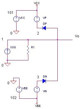
What's a common way to limit or clamp a circuit's maximum voltage swing? Simply hang a diode & voltage source from the supply rail. (See circuit above.) The circuit's operation is simple. Current source ISIG and resistor R1 develop a voltage signal. This voltage swings positive until diode DP begins to conduct through VP clamping the output voltage to
Vo_max = VCC - Vlimit
= VCC - (VP - Vd)
where Vd is the diode's ON voltage. As you can see, Vlimit is set by
Vlimit = VP - Vd
But how do we determine the diode's voltage? Recalling the Shockley diode equation, we write

where
Id - diode current
Vd - diode voltage
IS - diode saturation current
Vt - thermal voltage (constant)
Solving for Vd, we get
![]()
But, what is the maximum diode current Id? It's simply the maximum current expected out of source ISIG. Well, that's a good approximation, but not entirely true. A small current, Vo_max / R1, flows away from the diode through R1. Its good to check that this current is small compared to Id. If not, increase R1's value.
Finally calculate the voltage source
VP = Vlimit + Vd
(For the voltage limit during negative swings, the calculations are identical to the ones above.)
► EXCEL SPREADSHEET AND EXAMPLE
To help calculate component values, you can download an Excel spreadsheet V_Limit.xls. The example calculates the components for the following:
- Vlimit = within 1.5 V of the supply voltages
- Id = 1 mA max. ( Max Diode Current )
- IS = 1E-15 ( Diode Saturation Current )
Running through the spreadsheet, we get Vd = 0.714 V and VP = 2.214 V. This allows the output to swing to the rails within the following limit:
Vlimit = VP - Vd
= 2.214 V - 0.714 V
= 1.500 VWith a Vcc = 15 V, the output should clamp to 13.5 V.
CIRCUIT INSIGHT Take the SPICE file V_LIMIT.CIR out for a test run and plot V(1). ISIG generates a 1 mA peak sinewave current producing 1 mA x 100 k ohm = 100 Vpeak signal output. However, the voltage limit springs into action clamping the voltage to within 1.5 V of the 15 V rails or Vo_max = 13.5 V. How close to 13.5 V does the output swings. You might want to use the cursor of the your waveform viewer to get an accurate measure.
HANDS-ON DESIGN Choose different parameters like Vcc = 5 V and Vlimit =1 V. Design a new limiting circuit using the Excel spreadsheet and rerun the simulation. How close to 4 V does V(1) get clamped?
OP AMP MODEL WITH VOLTAGE CLAMP
Question: If an op amp model has additional frequency shaping stages, which stage is the best place for the voltage limiting circuit? Typically, the best location is the first gain stage. Why? The first gain stage typically contains all of the gain; the frequency shaping stages that follow are designed for a gain of 1. If the clamp resides at a later frequency shaping stage, the voltages in the first gain stage may swing hundreds or thousands of volts outside of the supply voltages.
Okay, time to strap the voltage limiting circuit onto the Intermediate op amp Model.
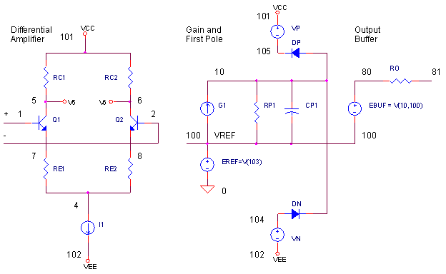
Let's design this voltage limiter for Vlimit = 1.5 V. So what is the maximum expected diode current? Remember that this op amp model is designed for a maximum current in G1 equal to the differential amplifier's bias current I1. For this particular model I1 = 1 mA. Similar to the Excel example above, we end up with VP and VN = 2.214 V.
VOLTAGE LIMIT TEST DRIVE
Are you ready to recklessly overdrive the op amp models input? Here's a non-inverting amplifier with a gain of 100 V/V.
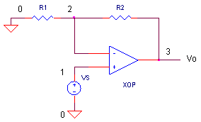
CIRCUIT INSIGHT
Run the SPICE file OPMODEL3_V_LIMIT.CIR. Does V(3) swing to within
1.5 V of the 15 V rails or Vo_max = 13.5 V ?
NOTE! You may not see the output clamped accurately as you might expect. The output will be attenuated by the op amp's output resistance working into the load and feedback resistors. To accurately check the clamp voltage, you might want to plot the subcircuit's internal node like 10 or 80 to get a better measure.
HANDS-ON DESIGN Pick a different supply rail and clamp voltage. Using the Excel spreadsheet, design a new clamp circuit and check if the circuit performs as you expect.
SIMULATION NOTES
Take a quick refresher tour of the
Intermediate Op Amp Model.
For a description of all op amp models, see
Op Amp Models.
For a quick review of subcircuits, check out
Why Use Subcircuits?
Get a crash course on SPICE simulation at
SPICE Basics.
A handy reference is available at SPICE
Command Summary.
To see how open-loop gain and bandwidth influence closed-loop bandwidth, see
Op Amp Bandwidth.
This model can be used with many of the op amp circuits available from the
Circuit Collection page.
SPICE FILES
Download the file or copy this netlist into a text file with the *.cir extension.
V_LIMIT.CIR - VOLTAGE LIMIT
*
* SUPPLIES
VCC	101	0	DC	15V
VEE	102	0	DC	-15V
*
* SINEWAVE - 1 MA PEAK x 100K = 100 V PEAK
ISIG	0	1	SIN(0 1MA 10KHZ)
R1	1	0	100K
*
* VOLTAGE LIMITING
DP	1	2	DLIM
VP	101	2	DC	2.214V
DN	3	1	DLIM
VN	3	102	DC	2.214V
*
.model	DLIM	D(IS=1E-15)
*
* ANALYSIS
.TRAN 	0.001MS  0.1MS
* VIEW RESULTS
.PRINT	TRAN 	V(1)
.PROBE
.END
Download the file or copy this netlist into a text file with the *.cir extension.
OPAMP3_V_LIMIT.CIR - OPAMP MODEL WITH OUTPUT VOLTAGE LIMITING
*
* SIGNAL SOURCE - TRIANGLE WAVE
VS	1	0	PWL(0MS 0V   25MS 1V  75MS -1V   100MS 0V)
*
* POWER SUPPLIES
VCC	10	0	DC	+15V
VEE	11	0	DC	-15V
*
R1	0	2	10K
R2	2	3	1000K
XOP	1 2 3  10 11	OPAMP3
*
*
* OPAMP MACRO MODEL (INTERMEDIATE LEVEL)
* WITH OUTPUT VOLTAGE LIMITING
*                IN+ IN- OUT  VCC  VEE
.SUBCKT OPAMP3   1   2   81   101   102
Q1	5 1	7	NPN
Q2	6 2	8	NPN
RC1	101	5	95.49
RC2	101	6	95.49
RE1	7	4	43.79
RE2	8	4	43.79
I1	4	102	0.001
*
* OPEN-LOOP GAIN, FIRST POLE AND SLEW RATE
G1	100 10	6 5 0.0104719
RP1	10	100	9.549MEG
CP1	10	100	0.0016667UF
*
* VOLTAGE LIMITING
DP	10	105	DLIM
VP	101	105	DC	2.214V
DN	104	10	DLIM
VN	104	102	DC	2.214V
.model	DLIM	D(IS=1E-15)
*
*OUTPUT STAGE
EOUT	80 100	10 100	1
RO	80	81	100
*
* INTERNAL REFERENCE
RREF1	101	103	100K
RREF2	103	102	100K
EREF	100 0	103 0 1
R100	100	0	1MEG
*
.model NPN  NPN(BF=50000)
*
.ENDS
*
* ANALYSIS
.TRAN 	1MS  100MS
*
* VIEW RESULTS
.PRINT	TRAN 	V(3)
.PROBE
.END
REFERENCES
SPICE-Compatible Op Amp Macro-Models, M. Alexander, D. Bowers, Analog Devices, Application Note AN-138, 1990.
© 2004 eCircuit Center