Intermediate Op Amp Model
CIRCUIT
 OPMODEL2.CR Download the
SPICE file
OPMODEL2.CR Download the
SPICE file
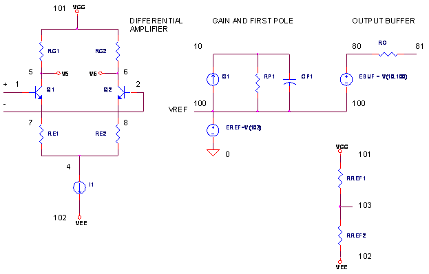
Just like the basic model, the intermediate opamp model captures your basic opamp stages: Differential Amplifier, Gain / Frequency Response and Output Buffer. However, this SPICE model is beginning to take the shape of those created by op amp manufacturers. Although each manufacturer has its own approach of modeling a particular behavior, most are based on this basic structure. And once you understand this model, you can easily customize or expand it to simulate other advanced op amp characteristics. There's also an Excel spreadsheet available below that calculates component values of the op amp circuit.
OP AMP BEHAVIORS
Here's a roundup of the behaviors modeled.
| Op Amp Behavior | Components | |
| Differential Amplifier | Q1, Q2, etc. | |
| Gain | G1, RP1 | |
| Single-Pole Frequency | RP1, CP1 | |
| Slew Rate | G1, CP1 | |
| Output Impedance | ROUT |
KEY FEATURES
This model, like many op amp models, has these key features.
» The voltage gain of differential amplifier and output buffer is unity.
» All of the voltage gain is provided by RP1 and G1.
» The current generated by G1 is the difference between collector currents in Q1 and Q2:
IG1 = IC1 - IC2.
OVERALL VOLTAGE GAIN
What's the overall gain of the circuit? From differential input to output buffer, you can write the gain as
Aol = KDIFF ∙ KG ∙ KBUFF
where
| Term | Stage | Voltage Gain | Comment | |
| KDIFF | Differential amp | RC1 / (RE1 + 1/gm) | Typically set to 1 | |
| KG | Voltage gain stage | KG1 ∙ RP1 | Set to the open-loop gain of the op amp. | |
| KBUFF | Output buffer | KEBUF | Typically set to 1 |
KG1 is the gain in A / V of G1, a Voltage-Controlled Current Source (VCCS).
KEBUF is the gain in V / V of EBUF, a Voltage-Controlled Voltage Source (VCVS).
Because a typical model sets KDIFF =1 and KBUFF=1, the open loop gain is simply
Aol = KG
= KG1 ∙ RP1
DIFFERENTIAL AMPLIFIER
What's different about this differential amplifier compared to the basic op amp model? This one uses an actual transistor differential pair in the first stage. Why? As you'll see later, it behaves much like the mechanism that causes slew-rate limiting inside an op amp. But first, let's look at the voltage gain from differential input to differential output.

where
gm = IE1 / VT
and VT = 25.85 mV at 27 ° C. Bias current I1 spits evenly into each emitter, IE1 = IE2 = I1 / 2, when the base voltages are equal. Typically, RC1 and RE1 are chosen for unity gain. This simplifies calculations. How? Conveniently, the open-loop gain, first pole and slew-rate are all now set by next stage's components - G1, RP1 and CP1.
FREQUENCY RESPONSE
The first-pole frequency fp1 provides the classic low-pass filter response of the op amp by itself. Modeled by a simple RC filter, CP1 and RP1, the frequency fp1 is given by
![]()
A direct result of fp1 and the open-loop DC gain AOL_DC is the Unity-Gain Frequency, fu – the frequency where AOL runs out of gas and falls to 1 V/V. It can be approximated by
fu = AOL_DC ∙ fp1
The Unity-Gain Frequency fu typically has another name, the Gain-Bandwidth Product. The higher the fu, the faster your op amp. Unfortunately, op amp manufacturers don't specify fp1. Fortunately, they do specify fu and Aol so you can easily calculate
![]()
SLEW-RATE LIMITING
What is slew-rate and why is it limited? Slew rate is simply how fast a voltage can change. And here's what limits it. In the voltage gain stage, G1's current charges CP1. This current in G1 is really the difference in the transistor collector currents. For large differential inputs, one transistor turns OFF completely while the other transistor turns ON completely. The ON transistor now carries the maximum current available, I1. This maximum current gets transferred to G1, limiting how fast CP1 gets charged. To a good approximation, this reflects the mechanism inside an op amp!
A current source charging a capacitor develops a voltage over time.
![]()
The rate of voltage change looks like this
![]()
For our op amp model, the rate is limited by the maximum transistor current available.
|
|
The remaining challenge is setting up G1's output to reflect the difference in collector currents! G1 generates a current controlled by the difference in collector voltages.
IG1 = KG1 ∙ ( V(5) - V(6) )
If RC1 = RC2, we can describe the voltage difference using collector currents.
V(5) - V(6) = RC1 ∙ ( IC1 - IC2 )
Sticking this into the previous equation gets us
IG1 = KG1 ∙ RC1 ∙ ( IC1 - IC2 )
Finally, by choosing
|
RC1 = 1 / KG1 |
G1's current becomes
IG1 = IC1 - IC2
OUTPUT BUFFER
The model for the output stage is a simple Voltage-Controlled Voltage Source (VCVS), whose output is described by
VEBUF = KEBUF ∙ ( V(10)-V(100) )
where KEBUF = 1. EBUF drives the output through series RO representing the op amp's output resistance. Although not very exciting, at this level of modeling anyway, far more interesting output models await in the Level 3 op amp model where advanced behaviors - current limiting, supply-rail current - will be created.
FLOATING INTERNAL REFERENCE
You may have noticed two of the stages, the Voltage Gain and the Output Stage, ride on top of a voltage source EREF at node 100. This voltage, named VREF, provides the internal reference for all stages in this model. It automatically "floats" the node midway between the supply rails. Resistors RREF1 and REF2, strung across the supply rails, develop this midpoint voltage at node 103.
EREF 100 0 103 0 1
RREF1 101 103 100K
RREF2 103 102 100K
Early op amp models did not have this midpoint voltage; all internal stages were referenced to 0V (ground). Although adequate for symmetric dual-supply applications, simulations may have been inaccurate for single, asymmetric, or unusual power supply configurations.
OP AMP SPECS TO COMPONENT VALUES
How do you go from op amp specs to SPICE model? Just a few simple calculations and your model is ready to go.
1. Choose the bias current I1 for the differential amp for a convenient value - possibly something less than the op amp's total quiescent current.
I1 = 1 mA, 100 uA or 10 uA, etc.
2. Calculate the components for slew rate
and the first-pole frequency.
You may need to calculate the fp1 from the op amp's DCGAIN and the Unity-Gain
Frequency fu (also equal to the Gain-Bandwidth Product GBP.)
3. The open-loop DC voltage gain is realized by
4. Make G1's current to be the difference in collector currents by choosing
5. The gain of the differential amp becomes unity if
where
gm = IE1 / VT = ( I1 / 2 ) / VT and VT = 25.85 mV at 27 ° C
WARNING! This op amp model works only if it passes the following test:
If Yes - GOTO simulation!
If No - Model can't handle it, needs to be modified first.
What happens? RE1 and RE2 become negative!
( See op amp with 2nd Gain Stage. )
6. Lastly, this model has an input bias current because of its transistor input stage. By setting the transistor's current gain β, you establish the input bias current Ibias.β = ( I1 / 2 ) / Ibias
The current gain β appears in the transistor model as parameter BF.
.model NPN NPN(BF=50000)
► EXCEL SPREADSHEET AND EXAMPLE
Okay, enough talk, let's build an op amp model. To help calculate the component values, you can download an Excel spreadsheet Opamp Parameters - Gain, Pole, Slew.xls. Based approximately on the specs of the classic 741 op amp, the spreadsheet should look like this.
| Enter | |||
| I1 (A) | 0.001 | Differential Amp Bias | |
| Slew (V/us) | 0.6 | Slew-Rate Limit | |
| fu (Hz) | 1.00E+06 | Unity-Gain Frequency (or Gain Bandwidth Product) | |
| Aol (V/V) | 100000 | Open-loop DC gain | |
| Vt (V) | 0.02585 | Voltage Constant | |
| Ibias (A) | 1.00E-08 | Input Bias Current | |
| Calculate | |||
| Ie1 (A) | 0.0005 | I1 / 2 | |
| fp1 (Hz) | 1.00E+01 | fp1 = fu / Aol | |
| TEST | 1.85E+05 | Slew-Rate / (4*pi*fp1*Vt) > Aol? | |
|
Yes - OK No - Model can't handle it. |
|||
| CP1 (uF) | 0.001666667 | CP1 = I1 / Slew | |
| RP1 (ohms) | 9.549E+06 | RP1=1/(2*pi*fp1*C1) | |
| KG1 (A/V) | 0.010471975 | KG1= Aol / RP1 | |
| RC1,2 (ohms) | 95.49 | RC1= 1 / KG1 | |
| RE1,2 (ohms) | 43.79 | RE1 = RC1 - 2*Vt / I1 | |
| BETA (A/A) | 5.00E+04 | BETA = Ie1 / Ibias |
OP AMP TEST DRIVE
OPEN-LOOP RESPONSE With no feedback components, let's try out the op amp model, OPMODEL2.CIR. For convenience, the model is defined as a subcircuit, OPAMP2. VS drives the positive input; R1 = 1 Ω grounds the negative input. Although not shown, this model needs its supply rails powered by VCC and VEE.
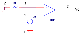
Run an AC Analysis and plot the output V(3). How does the SPICE model perform? Does the level at low frequencies meet the spec of AOL_DC = 100k V/V? Does the output fall to 0.707 of maximum at fp1 = 10 Hz? To get a better view, change the Y-Axis Settings to a log scale. And finally, does V(3) drop to unity at fu = 1MHz?
CLOSED-LOOP RESPONSE Time to wrap our op amp model inside some feedback and take it out for a spin.
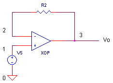
For a non-inverting amplifier with unity gain, remove R1 by adding a "*" at the beginning of its statement and add R2 = 1 Ω by removing the "*" at the beginning of its statement. VS generates a 1 V step input voltage. Run an Transient Analysis and plot the input V(1) and output V(3). How fast does the output reach 1 V?
CIRCUIT INSIGHT Does the slew-rate of this model max out at the expected 0.6 V/μs? The test is simple: did it take 1 μs for the output to reach 0.6 V? For larger input voltages like 5V, the slew-rate limit should remain the same. And so, regardless of the larger input, the output keeps chugging toward its final level at the same rate. During the slew-rate limited interval, check out peak current in G1 by plotting I(G1); it should be equal to I1 = 1 mA. This is the max current available to charge CP1.
For smaller input voltages - where the output does not exceed the slew-rate limit - the output settles quicker. Change VS to something smaller like 100MV. Did the circuit respond faster?
HANDS-ON DESIGN Add some gain by including R1 in the circuit. Or, change the circuit into an inverting amplifier. Vary the input voltage and gain. What happens to the output waveform and settling time?
OP AMP MODEL - LEVEL 3
If you made it through this op amp modeling adventure - congratulations! - a round of cool ones for everyone! Level 2 rounded up several key op amp behaviors, but left plenty of others behind. Next, we'll build up this model with advanced behaviors - one at a time - with the Level 3 op amp model.
Additional Frequency Shaping Stages
Output Voltage and Current Limit
Correct Supply Rail Current
Input Offset Voltage
Input Bias Current
CMR Frequency Response
Looking at the vast array of op amp models out there, it seems each manufacturer or SPICE modeler has their own idea of the "best" approach. We'll try to cover some of the more popular ones and capture, at least the spirit, of other approaches. Hopefully, it will give you the tools to understand existing models and create your own if needed.
SIMULATION NOTES
For a description of all op amp models, see
Op Amp Models.
To see how open-loop gain and bandwidth influence closed-loop bandwidth,
see Op Amp
Bandwidth.
SPICE FILE
Download the file or copy this netlist into a text file with the *.cir extension.
OPAMP2.CIR - OPAMP MODEL (LEVEL 2)
*
* SIGNAL SOURCE
VS	1	0	AC 1	PWL(0US 0V   0.01US 1V  100US 1V)
*
* POWER SUPPLIES
VCC	10	0	DC	+15V
VEE	11	0	DC	-15V
*
R1	0	2	1
*R2	2	3	1
XOP	1 2 3  10 11	OPAMP2
RL	3	0	100K
*
*
* OPAMP MACRO MODEL (INTREMEDIATE LEVEL)
*
*                IN+ IN- OUT  VCC  VEE
.SUBCKT OPAMP2   1   2   81   101   102
Q1	5 1	7	NPN
Q2	6 2	8	NPN
RC1	101	5	95.49
RC2	101	6	95.49
RE1	7	4	43.79
RE2	8	4	43.79
I1	4	102	0.001
*
* OPEN-LOOP GAIN, FIRST POLE AND SLEW RATE
G1	100 10	6 5 0.0104719
RP1	10	100	9.549MEG
CP1	10	100	0.0016667UF
*
*OUTPUT STAGE
EOUT	80 100	10 100	1
RO	80	81	100
*
* INTERNAL REFERENCE
RREF1	101	103	100K
RREF2	103	102	100K
EREF	100 0	103 0 1
R100	100	0	1MEG
*
.model NPN  NPN(BF=50000)
*
.ENDS
*
* ANALYSIS
.TRAN 	0.1US  5US
.AC 	DEC 	5 0.1 10MEG
*
* VIEW RESULTS
.PRINT	TRAN 	V(3)
.PRINT	AC 	V(3)
.PROBE
.END
REFERENCES
Macromodeling of Integrated Circuit Operational Amplifiers, G. Boyle, et al, IEEE Journal of Solid State Circuits, Vol SC-9, No. 6, December 1974.
SPICE-Compatible Op Amp Macro-Models, M. Alexander, D. Bowers, Analog Devices Application Note AN-138, 1990.
© 2003 eCircuit Center