Instrumentation Amplifier
Error Analysis
Step-by-Step
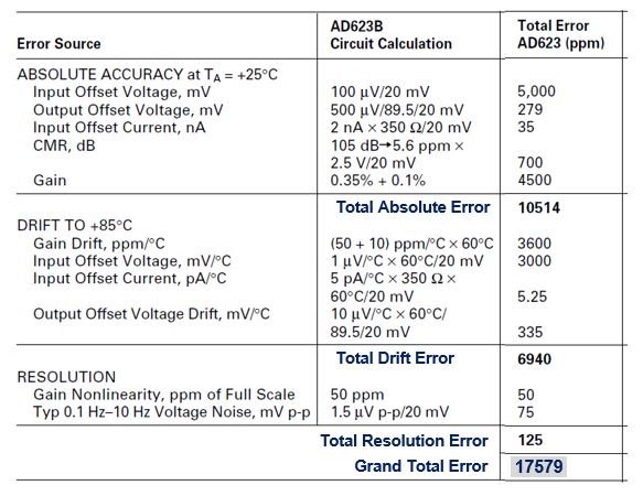
While the popular App Note AN-539 (Analog Devices) nicely describes and accounts for the AD623's errors, it's light on the theory and strategy behind the analysis equations. We'll do a teardown of this critical and challenging analysis. You'll get
- a step-by-step approach
- walk thru each error source
- derive the circuit and sensitivity equations
- separate errors into Gain / Offset, Calibratable / Uncalibratable
- an Excel file
- create, review and reuse with a systematic format
- vary parameters, see their effect on total error
- customize & expand template for your own designs
For Tutorials and more examples, see EBA Series
AN-539
You'll find excellent descriptions of the errors sources in this App Note from Analog Devices. The actual errors are tabulated for an easy read of the results. However, the calculations are inserted into the same table without much insight. This tutorial walks through each error in an easy step-by-step approach.
OFFSET AND GAIN ERRORS
What are the basic definitions for Offset and Gain Errors of an amplifier block?
- Ideal Amplifier with Gain K
- Vo = Vin*K
- Actual Amplifier with errors
- Vo = Vin* (K+∆K) + ∆Voffset
- ∆K - Gain Error
- change in Gain from ideal (K).
- also called Slope, Span error
- ∆Voffset - Offset Error
- change in offset from ideal (0V)
- also called Intercept, Zero Error
- Combined Offset and Gain Errors
- Error = ±∆Voffset + ( ±∆K x Reading )
MAX ERROR BUDGET
You can write the max error budget (or target spec) multiple ways. While not provided in the App Note, we'll specify a reasonable one for this analysis. Note: Sensor Full-Scale (FS) output = 20mV.
- ∆Voffset = 1.0% of FS + ∆K = 1.0% of Reading
- ∆Voffset = 0.2mV + ∆K = 1.0% of Reading
- ∆Voffset = 10,000ppm of FS + ∆K = 10,000ppm of Reading
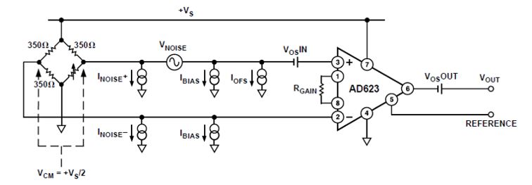
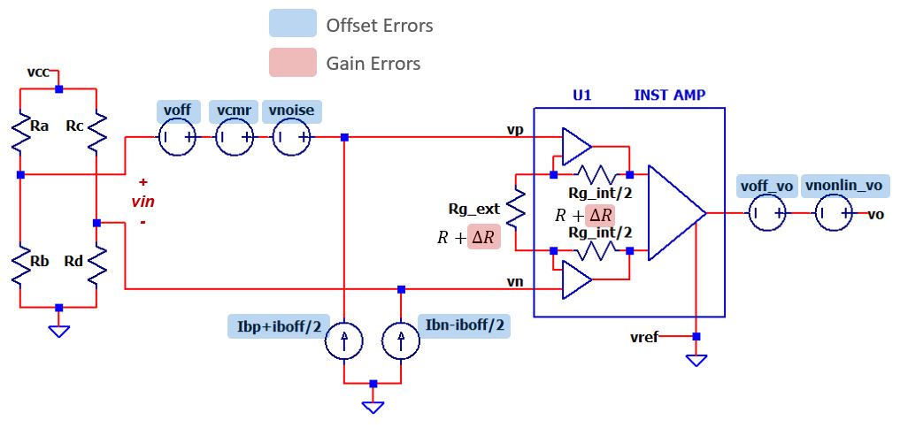
INSTRUMENTATION AMP
Schematic with Error Sources
Conditions and Assumptions
Temperature
- Ambient: Ta = 25C
- Max change: ∆T = 60C
Sensor
- Weigh Scale
- Full Scale (FS) Output = 20mV
- Sensor Bridge: Ra = Rb = Rc = Rd = 350 ohms,
- Assume ideal. no errors for amp analysis
Amplifier Device
- Analog Devices, AD623B
- Signal Gain: Rg_int / Rg_ext + 1
Errors
- Calibratable: Initial
- Un-calibratable: Drift, Noise, Non-linearity
- Errors will be Referred to Input (RTI)
- Errors totaled as Worst Case (sum absolute values)
- Low measure bandwidth: 10Hz
OFFSET ERRORS
The Inst Amp nicely showcases the analysis method for both input and output errors. The method also shows the approach for noise and non-linearity errors.
While the steps below may seem more detailed than needed for simpler errors, the value of creating a systematic approach can pay off when analyzing more complex, multi-stage designs.
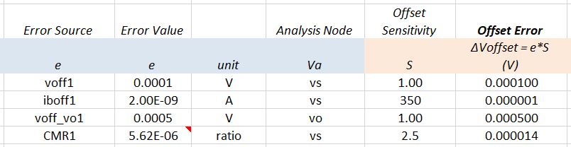
INPUT OFFSET VOLTAGE
| Description | Initial Errors | Drift Errors |
| Error Source: e | voff = 0.1mV | voff_TC = 1uV/C |
| Pick Analysis Node: Va | vp | vp |
| Calc Sensitivity: S How does e impact Va? | S = vp / voff = 1 | S = vp / voff = 1 |
| Calc Offset Error at Analysis Node Initial: ∆Voffset = e * S Drift: ∆Voffset = e * ∆T * S |
∆Voffset = 0.1mV * 1 |
∆Voffset = 1uV/C * 60C * 1 = 0.060 mV |
| Calc Gain from Input to Analysis Node: Ka = Va / Vin | Ka = vin/vp = 1 | Ka = vin/vp = 1 |
| Calc Error RTI (Referred-to-Input): ∆voffset_RTI = ∆voffset / Ka |
∆voffset_RTI = 0.1mV / 1 = 0.1mV |
∆voffset_RTI = 0.060mV/ 1 = 0.060mV |
OUTPUT OFFSET VOLTAGE
| Description | Initial Errors | Drift Errors |
| Error Source: e | voff_vo = 0.5mV | voff_vo_TC = 10uV/C |
| Pick Analysis Node: Va | vo | vo |
| Calc Sensitivity: S How does e impact Va? | S = vo / voff_vo = 1 | S = vo / voff_vo = 1 |
| Calc Offset Error at Analysis Node Initial: ∆Voffset = e * S Drift: ∆Voffset = e * ∆T * S |
∆Voffset = 0.5mV * 1 |
∆Voffset = 10uV/C * 60C * 1 = 0.60 mV |
| Calc Gain from Input to Analysis Node: Ka = Va / Vin |
Ka = vin/voff_vo = Rg_int / Rg_ext = 89.5 |
Ka = vin/voff_vo = Rg_int / Rg_ext = 89.5 |
| Calc Error RTI (Referred-to-Input): ∆voffset_RTI = ∆voffset / Ka |
∆voffset_RTI = 0.5mV / 89.5 = 5.6uV |
∆voffset_RTI = 0.6mV/ 89.5 = 6.7uV |
INPUT BIAS CURRENT
| Description | Initial Errors | Drift Errors |
| Error Source: e Bias currents are equal: ibp = ibn = ib With equal bridge Rs, errors cancel, but we'll show calculation. |
ib = 25nA | ib_TC = 25pA/C |
| Pick Analysis Node: Va | vp-vn | vp-vn |
| Calc Sensitivity: S How does e impact Va? |
S = (vp-vn) / ib = Ra||Rb - Rc||Rd = 175 - 175 = 0 |
S = (vp-vn) / ib = 0 |
| Calc Offset Error at Analysis Node Initial: ∆Voffset = e * S Drift: ∆Voffset = e * ∆T * S |
∆Voffset = 25nA * 0 = 0 |
∆Voffset = 25pA/C * 60C * 0 = 0 |
| Because error is zero we'll stop here. |
INPUT OFFSET BIAS CURRENT
| Description | Initial Errors | Drift Errors |
| Error Source: e | iboff = 2nA | iboff_TC = 5pA/C |
| Pick Analysis Node: Va | vp-vn | vp-vn |
| Calc Sensitivity: S How does e impact Va? |
S = (vp-vn) / iboff = 1/2*(Ra||Rb+Rc||Rd) = 1/2*(175+175) = 175 |
S = (vp-vn) /
iboff = 175 |
| Calc Offset Error at Analysis Node Initial: ∆Voffset = e * S Drift: ∆Voffset = e * ∆T * S |
∆Voffset = 2nA * 175 = 0.35uV |
∆Voffset = 5pA/C * 60C * 175 = 0.11uV |
| Calc Gain from Input to Analysis Node: Ka = Va / Vin | Ka = Vin/vp = 1 | Ka = Vin/vp = 1 |
| Calc Error RTI (Referred-to-Input): ∆voffset_RTI = ∆voffset / Ka |
∆voffset_RTI = 0.35uV / 1 = 0.35uV |
∆voffset_RTI = 0.11uV/ 1 = 0.11uV |
OUTPUT NON-LINEARITY
| Description | Calc Errors |
| Error Source: e (device spec at vo=4V) |
vnonlin_vo = 50ppm * 4V = 0.2mV |
| Pick Analysis Node: Va | vo |
| Calc Sensitivity: S How does e impact Va? | S = vo/vnonlin_vo = 1 |
| Calc Offset Error at Analysis Node: ∆Voffset = e * S |
∆Voffset = 0.2mV * 1 |
| Calc Gain from Input to Analysis Node: Ka = Va / Vin |
Ka = vin/vo = Rg_int/Rg_ex + 1 = 89.5 |
| Calc Error RTI (Referred-to-Input): ∆voffset_RTI = ∆voffset / Ka |
∆voffset_RTI = 0.2mV / 89.5 = 2.2uV |
INPUT VOLTAGE NOISE
| Description | Calc Errors |
| Error Source: e (device spec at 0.1 to 10Hz) |
vnoise = 2.5uVp-p = 1.25uVp |
| Pick Analysis Node: Va | vp |
| Calc Sensitivity: S How does e impact Va? | S = vp / vnoise = 1 |
| Calc Offset Error at Analysis Node: ∆Voffset = e * S |
∆Voffset = 1.25uVp * 1 = 1.25uV |
| Calc Gain from Input to Analysis Node: Ka = Va / Vin | Ka = vin/vnoise = 1 |
| Calc Error RTI (Referred-to-Input): ∆voffset_RTI = ∆voffset / Ka |
∆voffset_RTI = 1.25uV/1 = 1.25uV |
INPUT COMMON-MODE REJECTION ERROR
| Description | Calc Errors |
| Error Source: e | vcmr = vcm/CMRR = 2.5V/10105/20 = 14e-6 |
| Pick Analysis Node: Va | vp |
| Calc Sensitivity: S How does e impact Va? | S = vp/vcmr = 1 |
| Calc Offset Error ∆Voffset = e * S |
∆Voffset = 14e-6 * 1 = 14uV |
| Calc Gain from Input to Analysis Node: Ka = Va / Vin | Ka = vin/vcmr = 1 |
| Calc Error RTI (Referred-to-Input): ∆voffset_RTI = ∆voffset / Ka |
∆voffset_RTI = 14uV/1 = 14uV |
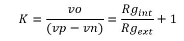
GAIN ERRORS
The differential signal gain is defined by
Gain errors often require more effort when calculating the Sensitivity S. You need to first write the gain equation and then apply calculus (Difference Method) to find S.
AN-539 skips the S calculation for gain altogether rounding it up to 1. But this only holds for high gain cases! For lower gains you could over estimate the Sensitivity (and Errors), so better to explicitly calculate S.
INTERNAL GAIN RESISTOR
| Description | Initial Errors | Drift Errors |
| Error Source: e | Rg_int_Tol = 0.35% |
Rg_int_TC = 50ppm/C = 0.0001%/C |
| Pick Analysis Node: Va | vo | vo |
| Calc Sensitivity: S How does e impact Gain K? Apply Difference Method: S = (∆K/K) / (∆R/R) where ∆K/K = (K'-K)/K |
K = Rg_int/Rg_ext+1 Rg_int = 100k Rg_ext = 1.13k K = 100k/1.13k+1 = 89.5 K'=100k*1.01/1.13k+1 = 90.4 ∆R/R = 0.01 S = (∆K/K) / (∆R/R) = +0.98 |
S = +0.98 |
| Calc Gain Error at Analysis Node Initial: ∆K/K = e * S Drift: ∆K/K = e * ∆T * S |
∆K/K = 0.35% * 0.98 = 0.34% |
∆K/K = 50ppm/C*60C*0.98 = 2940ppm = 0.29% |
| Gain errors can be referred to input node as-is, no RTI calc needed. |
EXTERNAL GAIN RESISTOR
| Description | Initial Errors | Drift Errors |
| Error Source: e | Rg_ext_Tol = 0.1% |
Rg_ext_TC = 10ppm/C = 0.0001%/C |
| Pick Analysis Node: Va | vo | vo |
| Calc Sensitivity: S How does e impact Gain K? Apply Difference Method: S = (∆K/K) / (∆R/R) where ∆K/K = (K'-K)/K |
K = Rg_int/Rg_ext+1 Rg_int = 100k Rg_ext = 1.13k K = 100k/1.13k+1 = 89.5 K'=100k/(1.13k*1.01)+1 = 88.6 ∆R/R = 0.01 S = (∆K/K) / (∆R/R) = -0.98 |
S = -0.98 |
| Calc Gain Error at Analysis Node Initial: ∆K/K = e * S Drift: ∆K/K = e * ∆T * S |
∆K/K = 0.1% * -0.98 = -0.099% |
∆K/K = 10ppm/C*60C*-0.98 = -593ppm = -0.059% |
| Normalized gain errors can be referred to input node as-is, no RTI calc needed. |
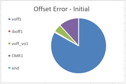
SUMMARY
Let's view the Gain & Offset errors as well which are Calibratable or not.
Description Error (V) (ppm) OFFSET INITIAL ( CALIBRATABLE ) Input Offset Voltage
Output Offset Voltage
Input Bias Current
Input Offset Bias Current
Input CMR100 uV
6 uV
0 uV
0.4 uV
14 uV5000
279
0
18
703OFFSET DRIFT, OTHER (UN-CALIBRATABLE) Input Offset Voltage Drift
Output Offset Voltage Drift
Input Bias Current Drift
Input Offset Bias Current Drift
Input Voltage Noise
Output Non-Linearity60 uV
7 uV
0 uV
0.1 uV
1 uV
2.2 uV3000
335
0
3
38
112GAIN INITIAL ( CALIBRATABLE ) Rg_int_Tol
Rg_ext_Tol0.35%
-0.098%3461
-979GAIN DRIFT, OTHER (UN-CALIBRATABLE) Rg_int_TC
Rg_ext_TC0.28 %
-0.059 %2966
-587
TOTALS
Errors are totalled as Worst Case (sum absolute values).
Total Error - No Cal
- Offset: 0.19mV (9507 ppm)
- Gain: 0.79% (7946 ppm)
- Combined: 17481 ppm
Total Error - With Cal (Drift, Other Errors only)
- Offset: 0.07mV (3490 ppm)
- Gain: 0.35% (3554 ppm)
- Combined: 7494 ppm
EBA WITH EXCEL
An Excel file was created to implement the error budget analysis.
- Organizes complex analyses into smaller managable sections
- Easier to create, review and debug
- Customizable and expandable to more complex circuits
- Modular for reuse in other designs
3 Worksheets
Worksheet Enter Calculate CIRCUIT CALC Circuit values Signal gains and error sensitivities OFFSET Offset error sources Offset errors and totals GAIN Gain error Sources Gain errors and totals
While 3 worksheets seems over-the-top for smaller circuits, you'll find a big advantage when analyzing more complex circuits or multi-stage systems!
The Excel file also creates a nice graph displaying error contributions at a glance.
Dive into the hands-on spreadsheet!
- Excel file:
Inst_Amp_AN-539_-_Error_Budget_Analysis.xlsx
Right Click on the filename, select "Save link as..." - Open file, explore the Circuit, Offset and Gain Sheets
- Play in the sandbox, modify values, see the impact on errors.
- Copy to a new file - experiment!
NOTES, IDEAS...
- The total error agrees closely with the original App Note. This analysis may be slightly more accurate by calculating a specific S for the gain resistors.
- To add another error source, simply add another row to the OFFSET or GAIN sheets.
- To add another stage, make a copy of the CIRCUIT CALC sheet and modify it for the new stage. Then add its error sources to the same OFFSET and GAIN sheets.
REFERENCES
- AN-539, Errors and Error Budget Analysis in Instrumentation
Amplifier Applications, Analog Devices Inc (ADI).
- AD623, Single Supply, Rail-to-Rail, Low Cost Instrumentation Amplifier, Datasheet, ADI.
- Tolerance Design of Electronic Circuits, Robert Spence, Randeep Soin, World Scientific Publishing.
Back to EBA Series