Differential Amp - Part 1
Offset Errors: voff, ib, iboff
Gain Errors: R1,
R2, R3, R4
The differential amplifier may appear only incrementially more complex than the basic op amp circuits. However, you'll discover the error analysis grows significantly more challenging. Part 1 breaks down the following errors into manageable concepts and steps.
- voff, Input Offset Voltage
- ib, Input Bias Current
- iboff, Input Offset Current
- R1-R4, Resistor Tolerance
Part 2 tackles the Common-Mode Offset Errors due to U1 (vcmr) and resistors (R1-R4).
We'll perform an analysis for each error. You'll get
- a step-by-step approach
- walk thru each error source
- derive the circuit and sensitivity equations
- an Excel file
- enter errors in a systematic format
- vary parameters, see their effect on total error
- customize & expand template for your own designs
For tutorials on Key Concepts and other circuits, goto EBA Series
OFFSET AND GAIN ERRORS
We'll start with basic error definitions of an amplifier block. What are Offset and Gain Errors?
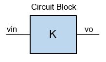
- Ideal Amplifier with Gain K
- Vo = Vin*K
- Actual Amplifier with errors
- Vo = Vin* (K+∆K) + ∆Voffset
- ∆K - Gain Error
- change in Gain from ideal (K).
- also called Slope, Span error
- ∆Voffset - Offset Error
- change in offset from ideal (0V)
- also called Intercept, Zero Error
- Combined Offset and Gain Errors
- Error = ±∆Voffset + ( ±∆K x Reading )
MAX ERROR BUDGET
The max budget (target spec) for amplifier has been chosen as:
- Offset Error: ∆Voffset = 2.5mV
- Gain Error: ∆K/K = 0.5% of Reading
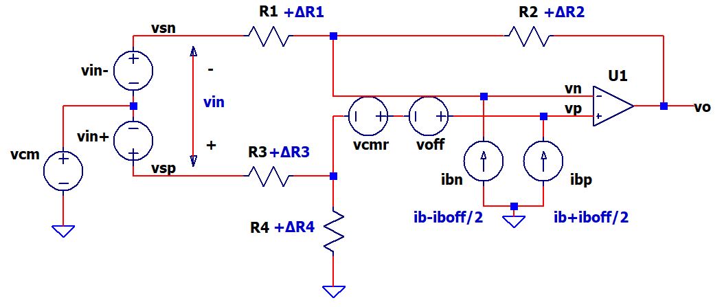
AMPLIFIER
Schematic with Error Sources
Here's a color map of the Offset and Gain Errors. Note how resistors R1-R4 contribute to both!
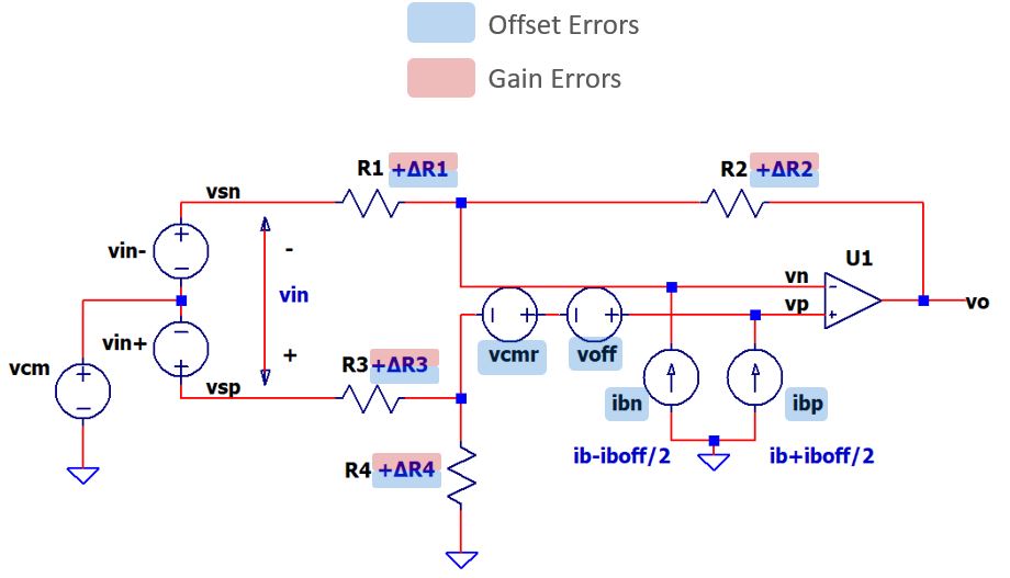
Error Sources
Description Initial Drift OFFSET ERRORS voff, Input Offset Voltage
ib, Input Bias Current
iboff, Input Offset Current0.1 mV
5 nA
5 nA10 uV / C
1 nA / C
1 nA / CGAIN ERRORS R1, Resistor Tolerance
R2, Resistor Tolerance
R3, Resistor Tolerance
R4, Resistor Tolerance0.1 %
0.1 %
0.1 %
0.1 %25 ppm / C
25 ppm / C
25 ppm / C
25 ppm / C
Conditions and Assumptions
Temperature
- Ambient: Ta = 25C
- Max change: ∆T = 30C
Amplifier
- vin = 100mV
- equal pos & neg signals
vin+ = 50mV, vin- = -50mV - see theory refresh for "Three Signal Types" below.
- equal pos & neg signals
- vcm = 5V
- R1=100k, R2=500k, R3=100k, R4=500k
- K = vo/vin = R2/R1 = +5.0
- vo = 100mV * 5 = 500mV
Errors
- All errors can be either polarity +/-.
- Errors will be Referred to Input (RTI)
- Errors totaled as Root Sum Square (RSS)
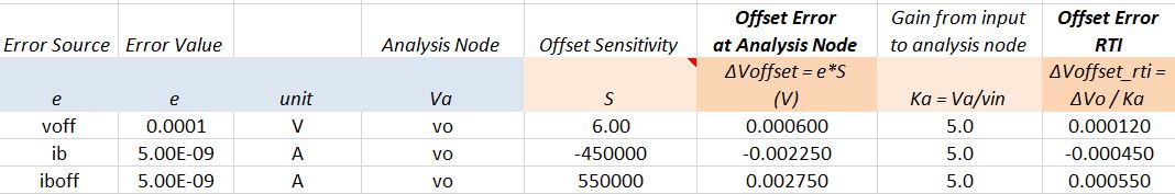
OFFSET ERRORS
While the steps may seem more detailed than needed for simpler errors, the value of creating a systematic approach will pay off when analyzing more complex, multi-stage designs.
INPUT OFFSET VOLTAGE
Because voff is modelled as voltage in series with the pos input, it gets amplified by the non-invertng gain.
| Description | Initial Errors | Drift Errors |
| Error Source: e | voff = 0.1mV | voff_TC = 10uV/C |
| Pick Analysis Node: Va | vo | vo |
| Calc Sensitivity: S How does e impact Va? |
S = vo / voff = R2/R1+1 = 6 |
S = 6 |
| Calc Offset Error at Analysis Node Initial: ∆Voffset = e * S Drift: ∆Voffset = e * ∆T * S |
∆Voffset = 0.1mV * 6 = 0.6mV |
∆Voffset = 10uV/C * 30C * 6 = 1.8 mV |
| Calc Gain from Input to Analysis Node: Ka = Va / Vin |
Ka = vin/vo = R2/R1 = 5 |
Ka = 5 |
| Calc Error RTI (Referred-to-Input): ∆voffset_RTI = ∆voffset / Ka |
∆voffset_RTI = 0.6mV / 5 = 0.12mV |
∆voffset_RTI = 1.8mV / 5 = 0.36mV |
INPUT BIAS CURRENT - Theory Refresh
The current into the pos / neg inputs has two components
ibp = ib + iboff / 2
ibn = ib - iboff / 2
where ib is the average of two currents
ib = (ibp + ibn) / 2
and iboff is the offset between the two currents
iboff = ibp - ibn
The output due to both ibp and ibn can be written
vo = ibp∙R3||R4∙(R2/R1+1) - ibn∙R2
Applying some math, we can find the Gain (Sensitivity) of vo to ib only
S = vo/ib = R3||R4∙(R2/R1+1) - R2
Similary, we can find the Gain (Sensitivity) of vo to iboff only
S = vo/iboff = ½ [ R3||R4∙(R2/R1+1) + R2 ]
INPUT BIAS CURRENT (ib)
The quick theory refresh (above) showed the Gain (Sensitivity) of vo to ib only
S = vo/ib = R3||R4∙(R2/R1+1) - R2
Let's walk through the error analysis.
| Description | Initial Errors | Drift Errors |
| Error Source: e | ib = 5nA | ib_TC = 1nA/C |
| Pick Analysis Node: Va | vo | vo |
| Calc Sensitivity: S How does e impact Va? |
S = vo / ib = Rs*(R2/R1+1)-R2 = -450k |
S = -450k |
| Calc Offset Error at Analysis Node Initial: ∆Voffset = e * S Drift: ∆Voffset = e * ∆T * S |
∆Voffset = 5nA * -450k = -2.25mV |
∆Voffset = 1nA/C*30C*-450k = -13.5mV |
| Calc Gain from Input to Analysis Node: Ka = Va / Vin |
Ka = vin/vo = R2/R1 = 5 |
Ka = 5 |
| Calc Error RTI (Referred-to-Input): ∆voffset_RTI = ∆voffset / Ka |
∆voffset_RTI = -2.25mV / 5 = -0.45mV |
∆voffset_RTI = -13.5mV / 5 = -2.7mV |
INPUT OFFSET CURRENT (iboff)
The quick theory refresh (above) showed the Gain (Sensitivity) of vo to iboff only
S = vo/iboff = ½ [ R3||R4 ∙ (R2/R1+1) + R2 ]
Let's walk through the error analysis.
| Description | Initial Errors | Drift Errors |
| Error Source: e | iboff = 5nA | ibp_TC = 1nA/C |
| Pick Analysis Node: Va | vo | vo |
| Calc Sensitivity: S How does e impact Va? |
S = vo / ib = ½ [R3||R4*(R2/R1+1) +R2] = 550k |
S = 550k |
| Calc Offset Error at Analysis Node Initial: ∆Voffset = e * S Drift: ∆Voffset = e * ∆T * S |
∆Voffset = 5nA * 550k = 2.75mV |
∆Voffset = 1nA/C*30C*550k = 16.5mV |
| Calc Gain from Input to Analysis Node: Ka = Va / Vin |
Ka = vin/vo = R2/R1 = 5 |
Ka = 5 |
| Calc Error RTI (Referred-to-Input): ∆voffset_RTI = ∆voffset / Ka |
∆voffset_RTI = 2.75mV / 5 = 0.55mV |
∆voffset_RTI = 16.5mV / 5 = 3.30mV |
GAIN ERRORS
Gain errors often require more effort when calculating the Sensitivity S.
You need to write the gain equation and then apply calculus (Difference
Method) to find S.
GAIN RESISTORS R1-R4 - Theory Refresh
With 4 resistor and two gain paths, the differential amplifier presents an analysis challenge.
What is the gain from the differential inputs to vo? By setting vcm = 0V, you can write the output as
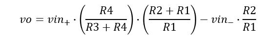
Assuming a bipolar input (vin+ = vin / 2, vin- = -vin /2) you can solve for the differential gain
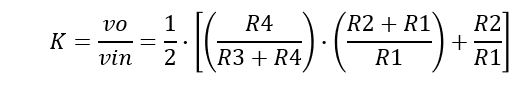
To make the calculations of Sensitivity (S) easier, let's rewrite the gain with fewer variables
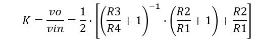
Also, by setting equal ratios R2/R1 = R4/R3, we get the familiar effective gain
K = vo/vin = R2 / R1
RESISTOR R3
As an example, we'll walk through the gain error contributed by R3.
To calculate Sensitivity, start with the ideal gain (K)
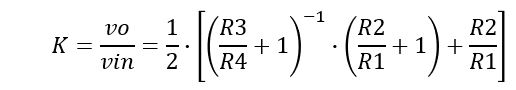
Increment R3 by a small ratio (say 1.01) to find it's impact on gain (K').
![]()
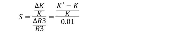
Calculate the Sensitivity of K to R3.
Finally calculate the actual gain error given R3's tolerance
![]()
Let's jump in with some numbers
| Description | Initial Errors | Drift Errors |
| Error Source: e | R3_Tol = 0.1% |
R4_TC = 25ppm/C = 25e-6/C |
| Pick Analysis Node: Va | vo | vo |
| Calc Sensitivity: S How does e impact Gain K? Apply Difference Method: S = (∆K/K) / (∆R/R) where ∆K/K = (K'-K)/K |
R1=R3=100k R2=R4=500k K = 5.000 K' = 4.996 ∆R/R = 0.01 S = (∆K/K) / (∆R/R) = -0.08 |
S = -0.08 |
| Calc Gain Error at Analysis Node Initial: ∆K/K = e * S Drift: ∆K/K = e * ∆T * S |
∆K/K = 0.1% * -0.08 = -0.008% |
∆K/K = 25e-6/C*30C*0.08 = -0.00006 = -0.006% |
| Normailzed gain errors can be referred to input as-is, no RTI calc needed. |
RESISTORS R1, R2, R4
For the remaining gain resistors, simply follow the basic method shown above for R3. Take each resistor, increment its value by 1.01 to find K', then calculate the Sensitivity as
S = (∆K/K) / (∆R/R)
= ((K'-K)/K) / 0.01
For the error results of all resistors, check out the hands-on
Excel file (see link below).
EBA WITH EXCEL
An Excel file was created to implement the error budget analysis.
- Organizes complex analyses into smaller managable sections
- Easier to create, review and debug
- Customizable and expandable to more complex circuits
- Modular for reuse in other designs
3 Worksheets
Worksheet Enter Calculate CIRCUIT CALC Circuit values Signal gains, levels and error Sensitivities OFFSET Offset error sources Offset errors and totals GAIN Gain error Sources Gain errors and totals
While 3 worksheets seems over-the-top for smaller circuits, you'll find a big advantage when analyzing more complex circuits or multi-stage systems!
Check out the easy entry (BLU col) and calculations (RED col) on the Offset Error sheet.
Explore the hands-on spreadsheet!
- Excel file: diff-amp1-a.xlsx
Right Click on the filename, select "Save link as...". - Open file, explore the Calc, Offset and Gain Sheets
- Play in the sandbox, modify values, see the impact on errors.
- Copy to a new file - experiment!
TRY IT!
- The total Offset Error (RSS) does not meet our spec of 2.5mV!
- How can you meet spec? Try lowering the R1,R2 values, by 5x or 10x. However, keep their ratio the same to mainitain the same gain.
3 SIGNAL TYPES - Theory Refresh
A differential amplifier can process a signal via three basic modes. What is the dominant signal paths(s) for each? Let's look at the three with typical appliations.
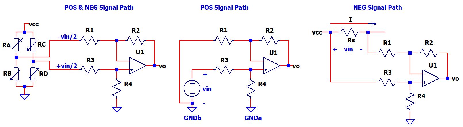
Suppose all cases measure a differential input of vin = 100mV. Keeping the differential gain equation in mind, we'll explore the signal pahs for all three cases. (Set vcm = 0V for analysis).
- Pos and Neg Signal Path
- A sensor bridge with 4 elements creates a changing signal on both pos and neg input paths with opposite polarities.
- vin+ = +50mV, vin- = -50mV
- Both sides of the gain equation influence Sensitivity and Gain error.
- Pos Signal Path
- A remote signal application measures vin referenced to GNDb at a different potential than GNDa. The signal changes at the Pos input (R3).
- vin+ = +100mV
- The Left side of the gain equation influences Sensitivity and Gain error.
- Neg Signal Path
- A high side current sensing application measures the voltage across the Rs. The signal changes at Neg input (R1).
- vin- = -100mV
- The Right side of the gain equation influences Sensitivity and Gain error.
Note: In all three modes, we analyzed the signals with vcm = 0. However, both Pos and Neg paths are needed to reject the actual Common-Mode signal.
For tutorials and other examples, goto EBA Series