Circuit Design
INTRO
As the late Jim Williams (renown analog designer) once said,
"Build the raft and start paddling...At some point the theorizing must stop
and you have to start actually doing something."
I found comfort and encouragement knowing that a seasoned designer could also feel hesitation wondering if their analysis and assumptions were sufficient to bring the abstract to life.
So, now it's time to render both the requirements and strategy into a real circuit.
Back to Design Series
BLOCK DIAGRAM
The high-level diagram shows us each block where we need to engineer the specific details with circuits, equations and components.
- Attenuator - scales 20V input to 4V for ADC.
- Filter - reduces 60Hz, clock and RF pickup.
- ADC - converts analog signal to Digital Word.
- Microcontroller - executes key hardware / software functions such as conversion, scaling, range selection and data transfer to PC.
SCHEMATIC
Given the Implementation Strategy as our guide, we fill in blocks above with schematic details.
DESIGN EQUATIONS
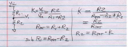
Part of the satisfaction (and frustration) of design is found in applying cool circuit theories. Often the basic equations require some exploring and solving for relevant forms for your design.

Adopt the powerful habit of grabbing a sheet of paper and a pencil. Good designers noodle regularly on pages full of circuits and equations. Practice this often - embrace a routine of trial / adjust / discover!
Check out several design equations for the voltmeter: DVM1_Design_Eqns.pdf.
INPUT ATTENUATOR
Two MOSFET switches select either a direct unity-gain connection (SW1) or the tap on a resistor divider (SW2). Driving digital outputs D12 or D13 to 0V will pull current through the LED, thereby turning on the switch.
SCHEMATIC
CIRCUIT REQUIREMENTS
- 4V Range: K=1
- 20V Range: K = 4V/20V = 1/5
- Rin = 1M both ranges
FUNCTION
Gain Conditions Analysis / Results 1 (4V Range) SW1=On
SW2=OffRin = R1 + R2
K = 11/5 (20V Range) SW1=Off
SW1=OnRin = R1 + R2
K = R2/(R1+R2)
R-DIVIDER DESIGN
- Requirements
- Gain: K = V1/Vin = 4V/20V = 1/5 = 0.2
- Input R: Rin = 1M both ranges
- Circuit Equations
- K = R2/(R1+R2)
- Rtot = R1+R2
- Design, Explore, Discover
- Solve 2 equations for R1 and R2 (may require paper+pencil)
- R2 = Rtot * K
- R1 = Rtot * (1-K)
- Calculate Power with Vmax = 50V (Overvoltage)
- P_R1 = V^2/R = (Vmax*(1-K))^2 / R1
- P_R2 = V^2/R = (Vmax*K)^2 / R2
- Excel Calculator DVM1_Circuit_Design1.xlsx (sheet: R-Divider)
- Choose components
- R1 - 806k, 1%, 1/10W, thru-hole resistor
- R2 - 200k, 1%, 1/10W, thru-hole resistor
OPTO SOLID-STATE-RELAYS (SSR)
- Component Type Selection
- Opto-isolated SSR
- Easy to drive LED with digital low (0V) and series R.
- High off-state voltage, low on-resistance, no supply needed.
- Requirements SW1, SW2
- On resistance: Ron < 10 ohms.
- Offstate Voltage: > 50V
- Choose Device
- TLP592A(F) Toshiba (existing stock)
- SSR RELAY SPST-NO 500MA 0-60V
- Ron = 2 ohms
- I_led > 3mA
- Vled = 1.1V at 3mA
- Circuit Equations
- Rled1 = (Vcc - Vled) / I_led
- Calculate Power of Rled
- P_Rled = Vled^2/Rled
- Excel Calculator DVM1_Circuit_Design1.xlsx (sheet: Opto RSS)
- Choose components
- RLED1,2 - 1k, 1%, 1/10W, thru-hole resistor
LOW-PASS FILTER
A filter reduces external noise sources (60 Hz mains, system clocks, radio frequencies, etc.) from corrupting the signal being digitized by the ADC.
SCHEMATIC
CIRCUIT REQUIREMENTS
- RC Low-pass filter
- 10x attenuation of a 60Hz mains pickup.
- Response time to accuracy < 1 sec.
DESIGN
- Circuit Equations
- Gain Magnitude: |H(f)| = 1 / (1 + (f/fc)2)1/2
- Gain above fc approx.: |H(f)| ≈ 1/(f/fc) = fc / f
- For 10x attenuation f = 60Hz
|H(f)| = 1/10 = fc / 60Hz
or fc = 60Hz*1/10 = 6 Hz - Tau = 1/(2*pi*fc)
- Choose RP1, calc CP1 = 1/(2*pi*Tau)
- Settling time to 1%. Ts = -ln(0.01)/ln(e)*Tau
- Excel Calculator DVM1_Circuit_Design1.xlsx (sheet: LP Filter)
- Choose components
- RP1 - 200k, 1%, 1/10W, thru-hole
- CP1 - 0.15uF, 10%, 100V, Ceramic, X7R, thru-hole
ADC CONVERTER
The development board (Arduino UNO R3) has been chosen for the project. A 10-bit ADC is included on the Microcontroller (Atmel ATmega328P). The accuracy has already been approved in the Implementation Strategy.
SCHEMATIC
CIRCUIT REQUIREMENTS
- ADC Resolution: 10-bits
- Input Range: 0 to 5V
- V Reference: Select AVCC +5V (Arduino default)
- Sample Time: 0.1s
DESIGN
- Circuit Equations
- Resolution: Vadc_res = Vref / 210
- Output: ADCword = Vadc / Vref * 210
- Input: Vadc = ADCword / 210 * Vref
- Conversion Time: Tsample = Ncycles * Tclk * Nprescaler
- Ncycles = required by ATmega328P for ADC conversion
- Tclk = ATmega328P clock period (Tclk = 1/fclk)
- Nprescaler = clock scaler in ADC module
- Excel Calculator DVM1_Circuit_Design1.xlsx (sheet: ADC)
ARDUINO INTERFACE
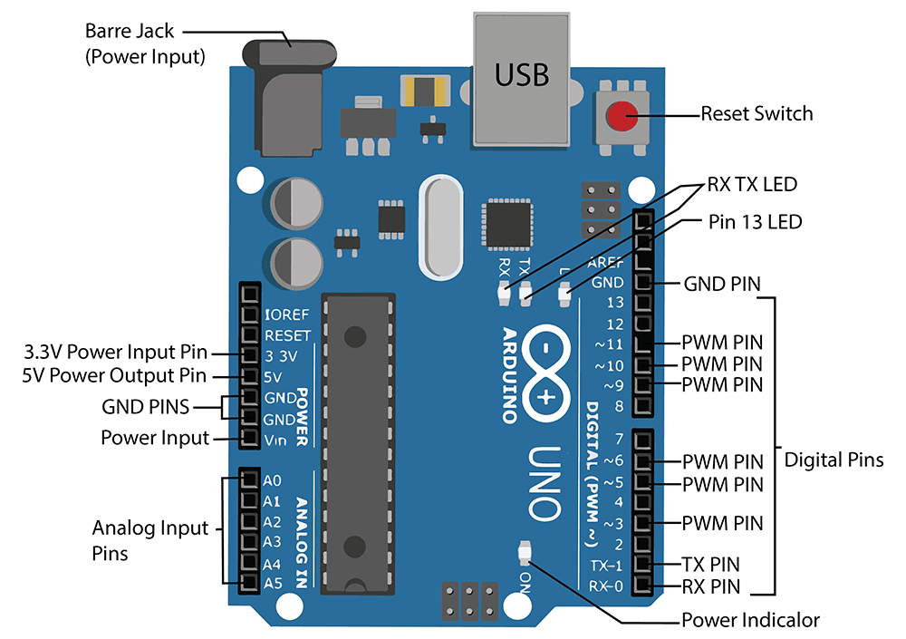
UNO R3 PINOUT

CIRCUIT CONNECTIONS
Type Signal Comment Power / Ground 5V
GNDPower for Opto-Relays and Pushbutton. Analog Inputs A0 Analog input voltage representing battery voltage. Digital Output D12
D13Digital outputs to drive 2 Opto-Relays SW1 and SW2. Digital Input D11 Digital input to read state of the pushbutton for V range select. PC Interface USB Power and programming capability from the PC.
ADC CONVERTER
The development board (Arduino UNO R3) has been chosen for the project. A 10-bit ADC is included on the Microcontroller (Atmel ATmega328P). The accuracy has already been approved in the Implementation Strategy.
HANDS-ON
Play in the Excel file - modify values, see what happens!
- Excel File: DVM1_Circuit_Design1.xlsx
- Right Click on the filename, select "Save link as...".
Input Range
- Suppose you needed to measure a 48V Battery? Pick a new Vrange such as 60V to replace the 20V range. What values of R1 and R2 are needed for your redesign?
Opto-Relay Drive
- You're asked to provide the LEDs with 5mA of drive current. What new value of Rled is needed?
Low-Pass Filter
- Turns out a major noise source is a nearby power supply radiating 120 Hz noise (full-wave rectified 60 Hz). Redesign the filter to reduce this noise frequency by 10x. What new values of fc and CP1 are required?
ADC Operation
- You'll test the basic ADC operation with a 1.5V battery connected. What digital vlaue do you expect when reading the ADC?
NEXT UP
To verify our Circuit Design, let's create a SPICE simulation.
Back to Design Series