Part 2
Single Potentiometer Cut & Boost Amp
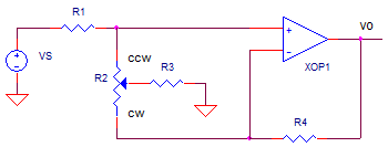
CIRCUIT
OP_CUT_BOOST.CIR Download the SPICE file
This topic continues a four part series in the design of a graphic equalizer circuit.
1. Band Cut & Boost - Series LCR
2. Cut & Boost - Single Pot
3. Band Cut & Boost - Series LCR and Pot.
4. Simulated Inductor and Graphic EQ
Part 2 of the Graphic Equalizer Series tackles the challenge of using a single potentiometer to achieve both a cut or a boost of the signal. The circuit may appear complex at first. But wait! Swinging the wiper to ether extremes reveals a straightforward operation.
CUT AND BOOST
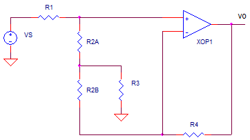
Let's push the potentiometer's wiper to both extremes and take a look at
the resulting circuits. First we'll redraw the circuit with the pot split
into R2A and R2B. Also keep in mind that R2 is chosen to be significantly
bigger than R1, R3 or R4.
Move the wiper fully Counter Clock Wise (CCW). This slides R3 up to R1 because R2A = 0. R2B has little effect on op amp gain because it's much bigger than R4. The circuit now looks like
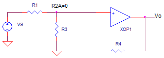
What remains is a simple attenuator R1, R3 followed by a unity gain buffer stage. The overall gain is less than 1 and you've got some "cut" behavior defined by
Kccw ≈ R3/(R1+R3)
Now move the wiper fully Clock Wise (CW). This slides R3 down to R4. Similarly, R2B has little effect on attenuation because it's much bigger than R1. The circuit looks like
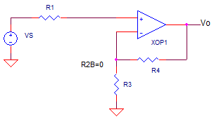
What remains is no attenuation of the input followed by a gain stage. The overall gain is greater than 1 and you've got "boost" defined by
Kcw ≈ (R3+R4) / R3
QUESTION: Now can you intuitively guess the gain when the wiper is positioned in the center? Let's see later in the simulation below.
CIRCUIT DESIGN
Let’s design the circuit for cut or boost of a about ten. This is easily
accomplished by choosing R1/R3 = R4/R3 = 10. Choosing R1 = R4 = 10k you get
R3 = 1k. As a rule of thumb choose, R2 (pot) to be 5 to 10 times larger than
R1. Choose R2 = 5 x R1 = 5 * 10k = 50k.
POTENTIOMETER SPICE MODEL
Although the potentiometer R2 appears as two separate resistors R2A and R2B,
it'd sure be nice having one control for both resistances.
* POTENTIOMETER POSITION (1=CCW, 50=MID, 99=CW)
.PARAM RPOS=50
*
R1 1 2 10K
R2A 2 3 { RPOS/100*50K }
R2B 3 4 { (1-RPOS/100)*50K }
The .PARAM let's you define a variable RPOS that takes on a value from 1 to 99. Now you can define R2A and R2B by equations that SPICE calculates on the fly before a simulation is run. For example, setting RPOS to a value of 1 (CCW position) results in
R2A = 0/100 x 50k ≈ 0 Ω
R2B = (1-0/100) x 50k ≈ 50 kΩ
Setting RPOS to a value of 50 (Center position) results in
R2A = 50/100 x 50k ≈ 25 Ω
R2B = (1-50/100) x 50k ≈ 25 kΩ
TEST DRIVE
VS drives the input with a 1V AC signal. Set RPOS Fully Counter
Clockwise (RPOS=1) for max attenuation. Run the file OP_CUT_BOOST.CIR to
perform an AC Analysis on the circuit.
CIRCUIT INSIGHT Check the frequency response by plotting the input V(1) and output V(5). Does the output show gain or attenuation? Does it cut the signal at about 10x (or -20dB)? Is the attenuation wideband or narrowband? With no tuned circuits, the attenuation should be flat from DC to above 100 kHz.
Now, set RPOS Fully Clockwise (RPOS=99) for max boost and rerun the simulation. Does it hit the design target of a boost around 10x (or +20dB)?
Finally, set RPOS to the center position (RPOS=50) and rerun the simulation. What do you think the response will be with the pot set dead center between cut and boost?
NEXT UP
The next piece of the Graphic EQ will take the first two parts and
combine them into a cut or boost that happens only over a narrow band of
frequencies..
SPICE FILE
Download the file or copy this netlist into a text file with the *.cir extention.
* OP_BOOST_CUT.CIR
*
VS	1	0	AC	1	SIN(0V 1V 800Hz)
*
* POTENTIOMETER POSITION (1=CCW, 50=MID, 99=CW)
.PARAM RPOS=50
*
R1	1	2	10K
R2A	2	3	{ RPOS/100*50K }
R2B	3	4	{ (1-RPOS/100)*50K }
R3	3	0	1k
R4	4	5	10k
* OPAMP
XOP1	2 4	5	OPAMP1
*
*
* OPAMP MACRO MODEL, SINGLE-POLE
* connections:      non-inverting input
*                   |   inverting input
*                   |   |   output
*                   |   |   |
.SUBCKT OPAMP1	    1   2   6
* INPUT IMPEDANCE
RIN	1	2	10MEG
* GAIN BW PRODUCT = 1MHZ
* DC GAIN (100K) AND POLE 1 (10HZ)
EGAIN	3 0	1 2	100K
RP1	3	4	1K
CP1	4	0	15.915UF
* OUTPUT BUFFER AND RESISTANCE
EBUFFER	5 0	4 0	1
ROUT	5	6	10
.ENDS
*
* ANALYSIS *************************************
*.TRAN 	1us  100us
.ac dec 40 10 100k
.PROBE
.END
© 2011 eCircuit Center