Op Amp Control - Lead Compensation
CIRCUIT

OP_CTRL_LEAD.CIR
Download the
SPICE file
OP_CTRL_LEAD_OL.CIR
Download the
SPICE file
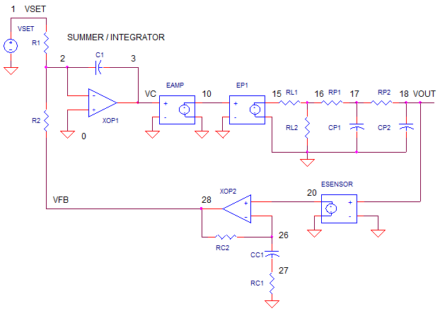
Let's start with a motor speed controller that's in trouble. The customer requests a fast response from the motor speed control system, but there's a big delay in the motor inertia and load. This causes huge overshoot and ringing which ends up shaking the system violently causing major damage.
A simple method to prevent oscillations reduces the bandwidth of the integrator. ( See Part 1 and Part 2.) Sure, you've stabilized the system, but at the expensive of having a slower response time. What if you need a faster response? By adding a simple circuit, you can tame a potentially unstable system and get it to respond quickly too.
LEAD COMPENSATION
In Part 2 we saw how time delays, or lags, can cause the system to ring and oscillate. What
does a time lag look like in the open-loop frequency domain? Delays
in the time domain add negative phase in the frequency domain.
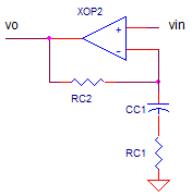
So what's the fix? One method uses lead compensation to add
positive phase back into the loop. Although there are several op
amp circuits that do the trick, here's a non-inverting version.

The lead compensator is defined by a lower frequency zero at fz and a higher frequency pole at fp.
fz = 1 / ( 2 · π · RC2 · CC1 )
fp = 1 / ( 2 · π · RC1 · CC1 )
It's frequency response has three distinct behaviors.
| Frequency Range | Gain | Phase | |
| f << fz | K = 1 (unity gain) |
0 | |
| fz < f < fp | Rising
+20 dB/dec |
Positive Phase (+90 deg max) |
|
| f > > fp | K = RC2/RC1+1 |
0 |
In theory, the zero behaves like a high-pass filter where the magnitude rises at +20 dB / dec with +45 deg at fz and up to +90 deg well above fz. However, the pole at fp acts like a low-pass filter where magnitude falls at -20dB/dec, cancelling out the zero making the response flat again at higher frequencies. Also, the pole adds negative 90 deg phase, canceling out the positive phase of the zero at f > fp. However, between fz and fp, you get a positive phase bump. This bump, when placed properly, can stabilize an otherwise ringing or oscillating response!
MOTOR CONTROLLER
The controller has a motor that spins at 100RPM per volt applied and
tachometer that produces 1V per 100RPM. The classic summer / integrator lies
at the heart of the controller.
CIRCUIT INSIGHT
Run a TRANSIENT RESPONSE of the system OP_CTRL_LEAD.CIR with RP1=RP2=100k and
CP1=CP2=0.1uF. The control components are R1=R2=100k and CINT=0.1uF. Set the
lead compensator to do nothing (unity gain) with RC2 = 10k, RC1=1k and CC1 =
1pF. Plotting the set command V(1) and feedback V(28) you can see the
response is anything but tame. Wild overshoot and ringing means poor speed
control and possible damage to motor / gears. Plot V(18) to see the actual
motor speed in RPM.
A simple way to stabilize the system is to slow it down (See Part 2). But faster responses call for more heroic design efforts
OPEN-LOOP ANALYSIS
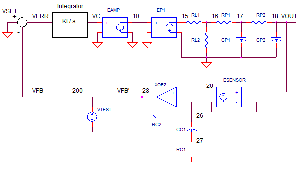
Why perform open-loop analysis? It opens a window into the nature of the
system not available otherwise. (Part 2 shows how
to break open the loop and model the system using classic control blocks.)

TROUBLE IN THE PLOTS Where are the signs of trouble? Run an AC RESPONSE of the open loop circuit OP_CTRL_LEAD_OL.CIR with RP1=RP2=100k and CP1=CP2=0.1uF. The control components are R1=R2=100k and CI=0.1uF. Initially, set the lead compensator to do nothing for now (unity gain) with RC2 = 100k, RC1=10k and CC1 = 1pF.
Plot the gain going around the loop, V(28/)V(200), and find where it falls to unity (0dB). What is the phase at this point? Yes, it's ugly - less than +20 deg (-340 deg) phase shift! Why is this bad? Remember, that an integrator controller starts with a phase around +90 deg (-270 deg); this is good . However, the negative phase of the delays can reduce this +90 deg down to 0 deg (-360) - a possible oscillator! The closer your phase to 0 (-360 deg) , the worse the response. Why? Because 0 deg (-360 deg) means the signal at V(28) is exactly in phase with signal at the start of the loop V(200). Consequently, the signal keeps adding to itself and growing to create a self sustained sine wave.
TUNE IT
Let's see
what power the lead compensator holds. One design / tuning technique requires a good guess
and some manual adjustment.
CIRCUIT DESIGN A reasonable guess places the zero at the unity gain frequency of the open loop plot, fz = fu. The plot of V(28)/V(200) shows an fu at about 10 Hz, therefore fz = fu = 10 Hz. Then choose the pole to be fp = fz · 10.
Choose fz = fu = 10Hz
Choose RC2 = 100k
Calc CC1 = 1/(2·pi·CC1·fz) = 0.159 uF (round down to 0.1 uF, a realistic value.)
Calc fp = 10 · fz = 10Hz · 10 = 100Hz
Calc RC1 = RC2 / 10 which places fp about 10 times higher than fz.
Then, you can manually change CC1 until you get a good response in the open and closed loop responses. (There are many different tuning methods. You can adjust it to better suit your system.)
Set CC1 = 0.1uF and run an AC response. To see the lead compensator only, add plot window and add the trace V(28)/V(20). You should see a nice positive phase bump between fz and fp. You should also see the gain rise as expected between these frequencies.
How did the lead compensator impact the open-loop response V(28)/V(200)? Yes, the phase has been increased from about 20 to about 50 deg at the unity gain frequency. This should have significant reduction in overshoot and preserve the fast rise time in the closed loop response.
CLOSED-LOOP TUNING
Now that you have an initial value for CC1, let's close the loop and
manually tune CC1 for an acceptable response.
CIRCUIT DESIGN With CC1 set to 0.1 uF, run a TRANSIENT RESPONSE of the closed-loop circuit OP_CTRL_LEAD.CIR. Plot the set command V(1) and feedback V(28). You should see the response has taken a turn for the better. It's not perfect, but much of the overshoot and ringing have been reduced. Okay, time for a bit of manual tuning. Start increasing or decreasing CC1 by factors of 2. Which direction takes you to a better response? Follow that direction, changing CC1 until you arrive at a response with a short rise time and minimal overshoot. Also, you'll find that adjusting the value further begin to worsen the response.
Congratulations, you've successfully applied lead compensation to meet the customer's requirements of a motor controller with a fast response time.
CLOSED-LOOP SPICE FILE
Download the file
or copy this netlist into a text file with the *.cir
extention.
OP_CTRL_LEAD.CIR
*
* SET POINT
VS	1	0	AC 1	PWL(0US 0V   0.01US -10V)
*
* CLASSIC CONTROL AMPLIFIER
R1	1	2	100K
R2	28	2	100K
CI	2	3	0.1UF
XOP1	0 2     3       op_001
*
* POWER AMP WITH LIMIT
EAMP	10	0	VALUE = {  LIMIT( 1 * V(3), +15, -15 )  }
*
* PROCESS (MOTOR, HEATER, ETC)
EP1	15	0	VALUE = { 100 * V(10)  }
* LOSSES (FRICTION, HEAT LOSS, ETC.)
RL1	15	16	0.1
RL2	16	0	100
* DELAY (INERTIA, THERMAL MASS, ETC.)
RP1	16	17	100K
CP1	17	0	0.1UF
RP2	17	18	100K
CP2	18	0	0.1UF
*
* SENSOR (TACHOMETER, THERMISTOR, ETC.)
ESENSE	20	0	VALUE = { 1/100 * V(18)  }
*
* LEAD COMPENSATION
CC1	26	27	0.1PF
RC1	27	0	10K
RC2	26	28	100K
XOP2	20  26  28   op_001

*
 * BASIC OP AMP MODEL
* Device Pins     In+ In- Vout
.SUBCKT op_001    1   2   82
RIN   1   2   1e9
*   Aol=1000000, fu=1000000 Hz
G1   0    10  VALUE = { 1.0 * V(1,2)  }
R1   10   0   1e6
C1   10   0   1.59e-7
* OUTPUT STAGE
EOUT 80 0   10  0    1
ROUT 80     82    10
.ENDS
*
* ANALYSIS *************************************
.TRAN 	0.1MS  400MS
*.AC 	DEC 	20 0.1 1000MEG
.PROBE
.END
OPEN-LOOP SPICE FILE
Download the file
or copy this netlist into a text file with the *.cir
extention.
OP_CTRL_LEAD_OL.CIR
*
* SET POINT
VS	100	0	AC 0
*
* INVERTER
EINV 1 0	100 0	-1
*
* OPEN-LOOP TEST VOLTAGE
VTEST	200	0	AC 1
*
* CLASSIC CONTROL AMPLIFIER
R1	1	2	100K
R2	200	2	100K
CI	2	3	0.1UF
XOP1	0 2     3       op_001
*
* POWER AMP WITH LIMIT
EAMP	10	0	VALUE = {  LIMIT( 1 * V(3), +15, -15 )  }
*
* PROCESS (MOTOR, HEATER, ETC)
EP1	15	0	VALUE = { 100 * V(10)  }
* LOSSES (FRICTION, HEAT LOSS, ETC.)
RL1	15	16	0.1
RL2	16	0	100
* DELAY (INERTIA, THERMAL MASS, ETC.)
RP1	16	17	100K
CP1	17	0	0.1UF
RP2	17	18	100K
CP2	18	0	0.1UF
*
* SENSOR (TACHOMETER, THERMISTOR, ETC.)
ESENSE	20	0	VALUE = { 1/100 * V(18)  }
*
* LEAD COMPENSATION
CCI	26	27	0.1PF
RC1	27	0	10K
RC2	26	28	100K
XOP2	20  26  28   op_001
*
*
*
 * BASIC OP AMP MODEL
* Device Pins     In+ In- Vout
.SUBCKT op_001    1   2   82
RIN   1   2   1e9
*   Aol=1000000, fu=1000000 Hz
G1   0    10  VALUE = { 1.0 * V(1,2)  }
R1   10   0   1e6
C1   10   0   1.59e-7
* OUTPUT STAGE
EOUT 80 0   10  0    1
ROUT 80     82    10
.ENDS
*
* ANALYSIS *************************************
*.TRAN 	0.1MS  1000MS
.AC DEC 20 0.01 1e5
.PROBE
.END
2011 eCircuit Center