Power Supply Bypassing
CIRCUIT
CBYPASS.CIR Download the SPICE file
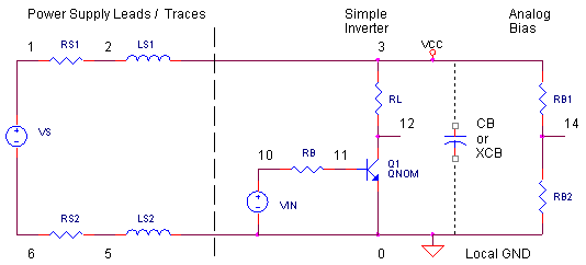
Its easy to take for granted. We place the power and ground symbols on a schematic page without considering how the power is delivered. But, there's more to it than just two symbols on a schematic. The figure above shows the real story of every circuit and its power source. Understanding the nature of power leads (or traces) is key to good circuit design.
SUPPLY LEADS
Power is delivered to your circuit from some remote location. The leads or traces that deliver the current possess two undeniable parasitic components: inductance and resistance. How much of the parasitic inductance can appear? Leads and traces can contribute up to 15 nH of inductance per inch. For a DC load this presents little problems. However, any circuit that demands a changing current can expect a voltage spike across the inductance given by the familiar equation
v = L di / dt
An example of a circuit that creates current transients is a simple transistor inverter Q1. When Q1 is off, there's no current drawn from the power supply. However, when Q1 turns on, the supply current changes from 0 to VCC / RL = 5 V / 200 Ω = 25 mA in 10 ns. The lead inductance responds to the current change with a voltage spike.
Not only can the inverter's performance be affected by the spike, but nearby analog circuits like the resistor divider RB1 and RB2 may also be degraded. For example, if the divider functions as threshold for a comparator input, a spike can cause false triggers. Or, if the divider biases a transducer, a spike will cause an error in the measurement.
CURRENT TRANSIENTS / VOLTAGE SPIKES
CIRCUIT INSIGHT Run a simulation of the file CBYPASS.CIR. Plot the Q1 output at V(12) and the local supply voltage V(3). What happens at V(3) every time the Q1 output switches on or off? The changing current demand from VS through LS1 and LS2 causes voltage spikes. To see the current drawn through the lead inductance LS1, add a new plot and the trace I(LS1). The current changes by 25 mA in about 10ns.
How do the voltage spikes effect nearby circuitry? Plot the resistor divider voltage at V(14). If this were the bias voltage for an analog circuit like a transducer, the measurement would be corrupted by the voltage transients at V(14).
BYPASS CAPACITORS
How can the voltage spikes be reduced? The solution is in a statement of wishful thinking: if only the fast current changes could be supplied to the circuit locally instead of remotely through LS1 and LS2. This local current source can be in the form of a capacitor CB between VCC and GND.
HANDS-ON DESIGN Add a 0.1uF bypass capacitor by removing the comment character "*" from the CB 3 0 0.1UF statement. Run a simulation and plot Q1 output V(12) and local supply voltage V(3). What happened to the voltage spikes? They should be dramatically reduced. Why? Capacitor CB now supplies most of the current transient; there is little current change through LS1 and LS2 to create voltage spikes. How does CB accomplishes this? During the demand of fast current transients, CB presents a lower impedance than LS1 and LS2. Add trace I(LS1) in a new plot window to see how its current transients have been reduced.
If you increased CB from 0.1 uF to 1.0 uF, CB supplies even more of the current demand locally, requiring even less from VS. At first it seems too good to be true; the larger the value of CB, the smaller the magnitude of the voltage spikes. However, real world capacitors have some disturbing similarities to the power supply leads as will be discussed in the next section.
PRACTICAL CAPACITORS
The bad news is that all real world capacitors have parasitic components similar to the power supply leads: inductance and resistance. What this means is that capacitors can actually be modeled by a series RLC circuit (See Capacitor Model for a review). The unexpected result is that the capacitor looks inductive at high frequencies! The switch from capacitive to inductive behavior happens at its self-resonant frequency. Your circuit may perform poorly if operating well above the capacitor's self-resonant frequency where the impedance rises inductively. (The good news is you can usually choose a capacitor whose reactance is still capacitive in your frequencies of interest.)
CIRCUIT INSIGHT
Remove CB from the circuit by adding a "*"
at the first character of the CB device statement. Now, add subcircuit XCB
that models a 1 uF bypass capacitor by removing the "*"
character
from the XCB 3 0
C105 statement. Run a simulation. Plot the Q1 output V(12)
and the local supply voltage V(3). What happened? The voltage spikes are
back! The reason is that the impedance of C105 becomes inductive and
begins rising at frequencies above self-resonance
(1 MHz). And our current spikes contain frequency components above 1 MHz.
Because C105's impedance is no longer small compared to LS1 and LS2, the
current spikes once again travel through the LS1, LS2 loop creating a voltage spikes.
SMALLER IS SOMETIMES BETTER
What we need is a capacitor with a higher self-resonant frequency. And the truth about capacitors is this: for a given capacitor type and package, smaller capacitor values generally have higher self resonant frequencies. So let's replace the 1uF model (C105) with the smaller 0.1 uF model (C104). Change the XCB subcircuit statement to look like XCB 3 0 C104.
CIRCUIT INSIGHT Run a simulation and plot Q1 output V(12) and local supply voltage V(3). The spikes have been reduced! Although capacitor model C104 has a smaller capacitor value than C105, it maintains a lower impedance at the frequencies of interest (the current spikes) because of its higher self-resonant frequency (10MHz).
SPICE FILE
Download the file or copy this netlist into a text file with the *.cir extention.
CBYPASS.CIR - POWER SUPPLY BYPASS CAPACITOR
*
* POWER SUPPLY
VS	1	6	DC	5
* POWER SUPPLY LEADS / TRACES
RS1	1	2	0.01
LS1	2	3	20NH
LS2	0	5	20NH
RS2	5	6	0.01
*
* SIMPLE INVERTER CIRCUIT
VIN	10	0	PULSE(0 5 0 10NS 10NS 90NS 200NS)
RB	10	11	5K
Q1	12	11 0	QNOM
RL	3	12	200
*
* ANALOG BIAS / REFERENCE VOLTAGE
RB1 	3	14	5000
RB2	14	0	5000
*
* BYPASS CAPACITOR
*CB	3	0	0.1UF
*XCB	3	0	C105
*
* 0.1 UF CAPACITOR MODEL - INCLUDES ESR AND SELF-RESONANCE
.SUBCKT C104	    1   4
* FO = 10 MHZ
C	1	2	0.1UF
R	2	3	0.08OHMS
L	3	4	2.53NH
.ENDS
*
* 1 UF CAPACITOR MODEL - INCLUDES ESR AND SELF-RESONANCE
.SUBCKT C105	    1   4
* FO = 1 MEG HZ
C	1	2	1UF
R	2	3	0.03OHMS
L	3	4	25.3NH
.ENDS
*
.model	QNOM	NPN
*
* ANALYSIS
.TRAN 1NS 200NS
* VIEW RESULTS
.PRINT	TRAN 	V(3) V(12) I(LS1)
.PLOT	TRAN 	V(3) V(12) I(LS1)
.PROBE
.END
© 2002-2003 eCircuit Center