Source Measure Unit (SMU)
Bandwidth & Settling Time
How to Calculate & Adjust SMU Speed
Download SPICE Netlist or LTSPICE
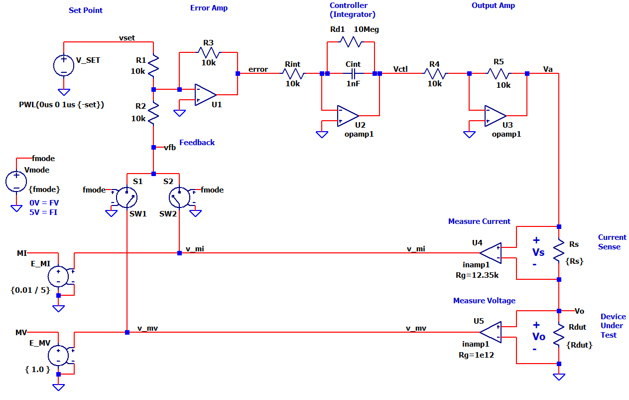
Schematic
Right Click on filename, select "Save link as..."
What settling time is needed for your SMU circuit to provide a precise
reading? What simple
formula relates the integrator response
and the overall SMU's bandwidth (settling time)?
What handy component in the circuit allows you to adjust the speed?
With some basic control theory, SPICE simulation and Excel Design file, you can develop some deeper understanding and intuition on this topic.
Back to SMU Series
GAINS AROUND THE LOOP
The SMU blocks shows the critical gains around the loop that will influence bandwidth. Review the basic blocks.

AMPLIFIER GAINS
Each amplifier gain will impact the bandwidth.
Kerr = Vctl / Verror = -(R3 / R2)
Kamp = Va / Vctl = -(R5 / R4)
Kmv = Vmv / Vo = (1 + 49.4k / Rg)
Kmi = Vmi / Vs = (1 + 49.4k / Rg)
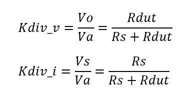
OUTPUT DIVIDER GAINS
The output resistor divider (Rs, Rdut) also impacts bandwidth. The divider ratio depends on the force mode (or feedback path): Kdiv_v for FV Mode, Kdiv_i for FI mode
CONTROL LOOP BANDWIDTH
How does the integrator's bandwidth relate to the overall system bandwidth?
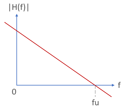
INTEGRATOR UNITY-GAIN FREQUENCY
Let's start with the Integrator's frequency response in the s-domain.
H(s) = Kint / s; Kint = 1/(Rint ∙ Cint)
Where is the frequency (fu) that the magnitude |H| falls to unity-gain (1) in the f domain?
| H(f) | = Kint / (2 ∙ π ∙ f)
| H(fu) | = Kint / (2 ∙ π ∙ fu) = 1
fu = Kint / (2 ∙ π)
Check out the frequency response plotted on log-log axes.
SYSTEM BANDWIDTH
A key relationship in control theory tells us that the System's bandwidth (fcl) is equal to the Integrator's unity-gain frequency (fu) scaled by the gains around the Loop.
FV Mode
fcl = fu ∙ Kerr ∙ Kamp ∙ Kdiv_v ∙ Kmv
FI Mode
fcl = fu ∙ Kerr ∙ Kamp ∙ Kdiv_i ∙ Kmi
(Note, this is generally true when the amplfier bandwidths are well above fu!)
SYSTEM RISE & SETTLING TIME
Given the system bandwidth (fcl), the output rise time to 63% of final value is:
tr63% = 1 / (2 ∙ π ∙ fcl)
For precision readings, what settling time allows output to fall within 1.0% and 0.1% of final value?
ts1.0% = 5 ∙ tr63%
ts0.1% = 7 ∙ tr63%
EXCEL FILE
Explore the hands-on spreadsheet with the bandwidth calculations!
- Excel file:
SMU-FVFI-circuit-1.xlsx
Right Click on filename, select "Save link as...". - Play in the sandbox, modify values, predict the impact on circuit!
- Copy to a new file - experiment!
SIMULATION
Let's take the SMU out for a speed test. For FV or FI mode, just enable / comment the relavant .PARAM statements:
- FV Mode, enable the SPICE directive:
.param fmode=0V FV=5V set=FV Rs=1k Rdut=20k
Comment out the FI params:
*.param fmode=5V ...
- FI Mode, enable the SPICE directive:
.param fmode=5V FI=0.01 set=FI/0.01A*5V Rs=100 Rdut=50
Comment out the FV params:
*.param fmode=0V ...
FV BANDWIDTH What is the expected bandwidth for the following Force Voltage test?
- COMPONENTS
- Rs = 1k, Rdut = 20k
- R1 = R2 = R3 = 10k
- Rint = 10k, Cint = 1nF
- R4 = R5 = 10k
- Rg(mv) = 1e12
- CALC GAINS
- Kerr = -R3/R2 = -1.0
- Kamp = -R5/R4 = -1.0
- Kdiv_v = Rdut/(Rs+Rdut) = 20k/(1k+20k) = 0.952
- Kmv = (1+49.4k/1e12) = 1.0
- CALC BANDWIDTH
- fu = 1 / (2 ∙ π ∙ Rint ∙ Cint) = 15.9 kHz
- fcl = fu ∙ Kerr ∙ Kamp ∙ Kdiv_v ∙ Kmv
= 15.9kHz ∙ 1.0 ∙ 1.0 ∙ 0.952 ∙ 1.0
= 15.2kHz - tr63% = 1/(2∙π∙fcl) = 10us
- ts1.0%= 5 ∙ tr63% = 50 us
Set the .PARAMs for FV mode and run a TRAN simulation of SMU-FVFI-ciruit-1.cir (or *.asc). Add traces -v(vset) and v(vfb). Does v(fb) rise to the 63.2% of 5V = 3.15V at 10us? Does the output settle to within 1% of final value at 50us?
What's a handy component to adjust speed? Increase the value of Rint by 2x. What will happen to the rise time? Rerun the sim with your adjusted Rint and find out!
What if you changed Rdut from 20k to 1k? Does Kdiv_v = Rdut/(Rs+Rdut) get bigger or smaller? What happens to the bandwidth?
FI BANDWIDTH What is the expected bandwidth for the following Force Current test?
- COMPONENTS
- Rs = 100, Rdut = 50
- R1 = R2 = R3 = 10k
- Rin = 10k, Cint = 1nF
- R4 = R5 = 10k
- Rg(mi) = 12.35k
- CALC GAINS
- Kerr = -R3/R2 = -1.0
- Kamp = -R5/R4 = -1.0
- Kdiv_i = Rs/(Rs+Rdut) = 100/(100+50) = 0.667
- Kmi = (1+49.4k/12.35k) = 5.0
- CALC BANDWIDTH
- fu = 1/(2 ∙ π ∙ Rint ∙ Cint) = 15.9 kHz
- fcl = fu ∙ Kerr ∙ Kamp ∙ Kdiv_i ∙ Kmi
= 15.9kHz ∙ 1.0 ∙1.0 ∙ 0.667 ∙ 5.0
= 53.1 kHz - tr63% = 1/(2∙π∙fcl) = 3.0 us
- ts1.0%= 5 ∙ tr63% = 15 us
Set the .PARAMs for FI mode and run a TRAN simulation of SMU-FVFI-ciruit-1.cir (or *.asc). Add traces -v(vset) and v(vfb). Does v(fb) rise to the 63.2% of 5V = 3.15V at 10us? Does the output settle to within 1% of final value at 15us?
What's a handy component to adjust speed? Increase the value of Rint by 2x. What will happen to the rise time? Rerun the sim with your adjusted Rint and find out!
What if you changed Rdut from 50 to 500? Does Kdiv_i = Rs/(Rs+Rdut) get bigger or smaller? What happens to the bandwidth?
SPICE NETLIST
Download SPICE Netlist or LTSPICE
Schematic
Right Click on filename, select "Save link as..."
* SMU-FVFI-circuit-1.cir
*
* Parameters
* FV Mode
.param fmode=0V FV=5V set=FV Rs=1k  Rdut=20k
* FI Mode
*.param fmode=5V FI=0.01 set=FI/0.01A*5V Rs=100 Rdut=50
*
* Set Point
V_SET vset 0 PWL(0us 0 1us {-set})
*
* Error Amp
R1 vset  N002  10k
R2 N002  vfb   10k
R3 error N002  10k
XU1 N002 0 error opamp1
*
* Controller (Integrator)
Rint N001  error 10k
Cint Vctl  N001  1nF
Rd1  Vctl  N001  10Meg
XU2 N001 0 Vctl opamp1
*
* Output Amp
R4  N003   Vctl  10k
R5  Va     N003  10k
XU3 N003 0 Va opamp1
*
* Current Sense
Rs  Va     Vo   {Rs}
*
* Device Under Test
Rdut Vo    0    {Rdut}
*
* INST AMP MI
XU4 Vo Va v_mi  inamp1 Rg=12.35k
*
* INST AMP MV
XU5 0 Vo v_mv  inamp1 Rg=1e12
*
* Measure Voltage and Current
E_MV  MV 0  v_mv 0  { 1.0 }
E_MI  MI 0  v_mi 0  {0.01 / 5}
*
* Force Mode
Vmode fmode 0 {fmode}
*
* Feedback Mux
S1  v_mv vfb   fmode 0   SW1
S2  v_mi vfb   fmode 0   SW2
*
* Simulation
.tran 200us
*
* Opamp Model ******************************
*  pin order      in- in+ out
.SUBCKT OPAMP1    1  2   3
EGAIN     3 0   2 1     1000K
.ENDS
*
* Inst Amp Model **************************
*  pin order      in- in+ out
.SUBCKT INAMP1    1  2   3
EGAIN     3 0    value={ (V(2)-V(1)) * (1+49.4k/Rg) }
.ENDS
*
* Switch Models **************************
.model SW1 SW(Ron=1 Roff=1Meg  Von=0V Voff=5V )
.model SW2 SW(Ron=1 Roff=1Meg  Von=5V Voff=0V )
*
.end
Back to SMU Series