Frequency Shaping
CIRCUIT
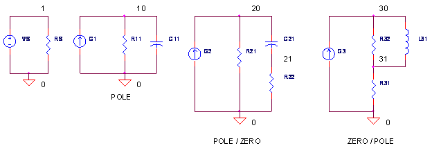
POLE_ZERO_STAGES.CIR Download the SPICE file
OPMODEL3_FREQ_SHAPING.CIR Download the SPICE file
Up to this point, Level 1 and 2 opamp models have simulated only single-pole frequency responses (a simple low-pass filter). But in reality, more poles may lurk at higher frequencies. Why bother simulating them? Higher poles can spell trouble by adding phase (or time-delay) at the output, pushing your amplifier toward ringing, overshoot and possibly oscillation. And your simulation won't show these danger signs if your models don't capture the whole frequency response story. But help is on the way! Adding frequency shaping stages to your op amp - or any other SPICE model - is rather simple. And to help you zip through the component calculations, there's an Excel Spreadsheet available you can download.
FREQUENCY SHAPING STAGES
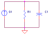
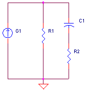
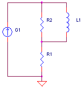
Here are several handy frequency shaping circuits for your op amp model. You can add a variable yet unlimited number of stages without having to start the model from scratch. What makes this possible? Each stage has two key features - they are DC coupled and have unity gain at DC. As a result, you can tweak your high frequency response without having to mess around with the initial DC Open Loop Gain, First-Pole Frequency or Slew Rate components.
Voltage Controlled Current Sources (VCCS) we're chosen to create the stages (they could have created with voltage sources as well.) To get the desired unity gain, set the current source gain KG1 equal to the DC resistance, KG1 = 1 / R1. Although the initial choice of R1 arbitrary, try to keep its value in the range of other components in the circuit.
|
POLE STAGE
|
 |
 |
|
||
|
POLE / ZERO STAGE fp < fz
|
 |
 |
|
||
|
ZERO / POLE STAGE fz < fp
|
 |
 |
|
There's an Excel Spreadsheet available, POLE_ZERO_STAGES.XLS, that calculates the RC component values based on your desired pole and zero frequencies.
CIRCUIT INSIGHT Let's shape and sculpt the spectrum a bit with the SPICE file - POLE_ZERO_STAGES.CIR. Voltage source VS drives three different frequency shaping stages - a pole, pole/zero and zero/pole stage. Common to all stages is a pole or zero frequency at 100 Hz. So from DC to 100 Hz they all cruise along at unity gain. However, above 100 Hz, the outputs begin to diverge. Check out the responses by plotting V(10), V(20) and V(30). To get a better view, change the Y axis to a log scale.
What do you notice about these responses? Above 100 Hz all responses rise or fall by a factor of 10 for every factor of 10 increase in frequency. Or stated in the familiar decibel lingo, the responses rise or fall by 20 dB / decade (derived from 20∙log10 = 20 dB). This leads to another observation - the gain changes by the same ratio as the ratio of pole/zero frequencies. Amazing but true, for fz / fp = 100, the gain should change by the same ratio.
HANDS-ON DESIGN Pick several new pole and zero frequencies. Crank out your new component values using the Excel spreadsheet and simulate the new spectrum.
OP AMP MODEL WITH MULTIPLE POLES
Okay, let's bolt a few of these frequency shaping stages onto an op amp and see what happens. Suppose an op amp has a unity gain frequency of about 50 MHz (AOL_DC=100 kV/V and fp1=500 Hz). But, that's not the whole story. There's a couple of high frequency poles at 100 MHz. No problem, you might say. This is beyond 50MHz, why worry about it? Unfortunately, the negative phase of poles begin to show well before the actual pole frequency. And accumulating negative phase at the unity gain frequency, typically brings bad news in a feedback system.
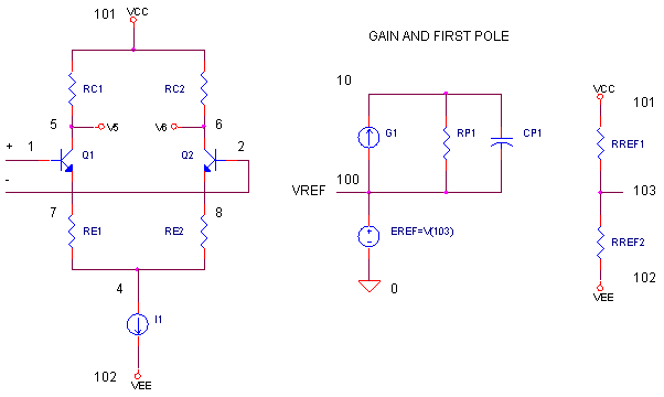

OPEN-LOOP RESPONSE Let's have a quick look at this op amp, OP3_FREQ_SHAPING.CIR, with no feedback components. VS drives the positive input; R1 = 1 Ω grounds the negative input.
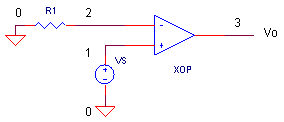
Run an AC Analysis and plot the output VM(3) (setting the Y-axis to a log scale helps!) Now, open a separate window and check out the phase, VP(3). As you recall, the danger zone of a feedback system is the following condition: unity gain and a phase shift of -180 ° in the open-loop circuit. The phase drops to -90° (due to the first pole) until about 1MHz. Now the phase begins to fall quickly toward -180° (due to the two poles at 100 MHz). This situation is typical of many op amps. And the closer to -180° the phase gets, the worse the overshoot and ringing will be.
CLOSED-LOOP RESPONSE Okay, let's close the loop and put the amplifier to the test.
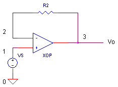
For a non-inverting amplifier with gain = +1, remove R1 by adding a "*" at the beginning of its statement and add R2 = 1 Ω by removing the "*" at the beginning of its statement. VS generates a 1 V step input voltage.
CIRCUIT INSIGHT Run a Transient Analysis and plot the input V(1) and output V(3). As expected the output rings and overshoots, but how bad is it? It ain't pretty, but it settles within 100 ns or so depending on your accuracy needed. Let's step back for moment - what if the two poles at 100 MHz were not included? Temporarily comment out CP2 and CP3 and check out the response. Nice, isn't it? We could have easily been lulled into design bliss by ignoring the poles, only to be surprised (and confused) when the actual circuit was tested!
Want to make matters worse? Just hang a capacitor of 10 pF or so at the output. As you might guess, the capacitor forms a low-pass filter (pole) with the output resistance of the op amp. This only adds more negative phase edging the total toward -180°. For those who like to push the limits, keep adding capacitance. At some point this amplifier becomes a useless collection of ringing components.
OP AMP PARAMETERS
So far we've avoided the trickiest part of shaping the op amp frequency response. Where do the pole / zero locations come from? Unfortunately, most op amp data sheets don't explicitly list them. But the information is usually there, implicit in the magnitude and phase graphs of the open-loop frequency response. So your challenge lies in sculpting and tweaking the spectrum, adding poles and zeros until it matches reality. Will it be perfect? Probably not. But, at least your circuit's response will raise a flag, warning of potential overshoot and ringing.
There's another way to get the op amp poles and zeros. Many manufacturers create SPICE models that explicitly list the frequency locations. You now have the choice of using the manufacturer's model or creating your own. Many times, I'll create my own if I don't need all of the functions from the manufacturer's model or I'm using an evaluation version of SPICE that doesn't support larger models.
SIMULATION NOTES
For a description of all op amp models, see
Op Amp Models.
For a quick review of subcircuits, check out
Why Use Subcircuits?
Get a crash course on SPICE simulation at
SPICE Basics.
A handy reference is available at SPICE
Command Summary.
This op amp model can be used for many of the op amp
circuits available from the Circuit
Collection page.
SPICE FILES
Download the file or copy this netlist into a text file with the *.cir extension.
POLE_ZERO_STAGES.CIR - POLE / ZERO COMBINATIONS
*
* SIGNAL SOURCE
VS	1	0	AC	1V
*
* POLE
G1	0 10	1 0	1U
R11	10	0	1MEG
C11	10	0	1.59NF
*
* POLE / ZERO
G2	0 20 1 0	1U
R21	20	0	1MEG
C21	20	21	1.58NF
R22	21	0	10.1K
*
* ZERO / POLE
G3	0 30	1 0	1U
R31	30	31	9MEG
L31	30	31	1432H
R32	31	0	1MEG
*
* ANALYSIS
.AC	DEC	5	1HZ	1MEGHZ
*
* VIEW RESULTS
.PRINT	AC 	VM(10) VM(20) VM(30)
.PROBE
.END
Download the file or copy this netlist into a text file with the *.cir extension.
OPMODEL3_FREQ_SHAPING.CIR - OPAMP MODEL (LEVEL 3) WITH 2 ADDITIONAL POLES
*
* SIGNAL SOURCE
VS	1 0	AC 1   PWL(0US 0V  1NS 0.1V  200NS 0.1V  201NS 0V  400NS 0V)
*
* POWER SUPPLIES
VCC	10	0	DC	+15V
VEE	11	0	DC	-15V
*
R1	0	2	1
*R2	2	3	1
XOP	1 2 3  10 11	OPAMP3
RL	3	0	100K
*CL	3	0	80PF
*
*
* OPAMP MACRO MODEL - LEVEL 3 WITH ADDITIONAL FREQUENCY SHAPING
*
* AOL_DC = 100K, FP1 = 500HZ, SLEW = 20 V/US
* 2 ADDITIONAL POLES AT 100MHZ
*
*
*                IN+ IN- OUT  VCC  VEE
.SUBCKT OPAMP3   1   2   81   101   102
Q1	5 1	7	NPN
Q2	6 2	8	NPN
RC1	101	5	63.66
RC2	101	6	63.66
RE1	7	4	11.96
RE2	8	4	11.96
I1	4	102	0.001
*
* OPEN-LOOP GAIN, FIRST POLE AND SLEW RATE
G1	100 10	6 5 0.015707
RP1	10	100	6.366MEG
CP1	10	100	0.00005UF
*
* 2ND POLE 100MHZ
G2	100 20	10 100 0.01
RP2	20	100	100
CP2	20	100	15.9PF
*
* 3RD POLE 100MHZ
G3	100 30	20 100 0.01
RP3	30	100	100
CP3	30	100	15.9PF
*
* OUTPUT STAGE
EOUT	80 100	30 100	1
RO	80	81	50
*
* INTERNAL REFERENCE
RREF1	101	103	100K
RREF2	103	102	100K
EREF	100 0	103 0 1
R100	100	0	1MEG
*
.model NPN  NPN(BF=50000)
*
.ENDS
*
* ANALYSIS
.TRAN 	0.001US  0.4US 0 0.001US
.AC 	DEC 	5 10HZ 100MEGHZ
*
* VIEW RESULTS
.PRINT	TRAN 	V(3)
.PRINT	AC 	V(3)
.PROBE
.END
© 2003 eCircuit Center
