Common-Mode Rejection (CMR)
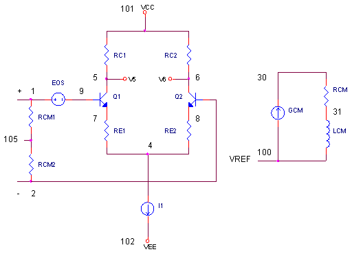
CIRCUIT


OPMODEL3_CMR.CIR Download the SPICE file
Ideally, an op amp should
► Respond only to differential inputs.
► Ignore voltages common to both inputs.
The keyword here is "should." While real op amps do a fantastic job of rejecting voltages common to both inputs - it's not perfect. A small output results from a change in input common-mode voltage. What causes this output? Due to mismatching in the transistors and resistors of the input stage, the common-mode voltage produces a small differential error voltage at the input terminals. Subsequently, this error gets amplified right along with any other signal appearing at the input. But, how does the common-mode error behave versus frequency? And how do we include this error in an op amp SPICE model?
COMMON-MODE REJECTION RATIO
The first step in developing a SPICE model for CMR is understanding an op amp's Common Mode Rejection Ratio (CMRR). The CMRR is a measure of how well the device rejects a common-mode signal.
![]()
Its simply the ratio of the differential gain Av over the common-mode gain Acm.
| Differential Gain | Common-Mode Gain | |
| Av = Vo / (v+ - v-) | Acm = Vo / Vcm | |
| This is
your basic open-loop gain of an op amp. |
Here's the gain with
the inputs tied together at Vcm = v+ = v-. |
Let's see if the CMRR equation can give us some insight. Substituting the gains above into CMRR will get us

Rearrange it a little and we get
![]()
This equation tells us a nice story - how much of a differential error voltage is produced at the input given Vcm and the device's CMRR! We can use this directly to develop a SPICE model.
CMR SPICE MODEL
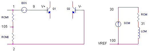
To model an op amp's CMRR, we just add a few components.

* CMR COMPONENTS
RCM1 1 105 1000MEG
RCM2 2 105 1000MEG
EOS 1 9 POLY(1) 30 100 0 1
*
* CMRR - DC AND 1ST POLE
GCM 100 30 105 100 1E-11
RCM 30 31 1MEG
LCM 31 100 159
Common-Mode Voltage - Vcm Vcm is determined by RCM1 and RCM2 strung between the inputs terminals. This divider calculates the average of the input voltages.
![]()
Vcm is actually the difference between this average and the internal reference voltage at V(100).
Vcm = V(105) - V(100)
RCM1 and RCM2 should be large enough such that they don't effect the input impedance of the op amp.
CMRR Next, we include a stage with a "gain" of 1/CMRR. GCM forces a current, based on Vcm, through RCM to get the common-mode error voltage at V(30,100).
V(30,100) = ( V(105) - V(100) )
∙ 1/CMRR
= ( V(105) - V(100) ) ∙
KGCM ∙ RCM
Now, we just need to inserting this error voltage into the input terminals. EOS places the error voltage at the positive input terminal with a gain of 1.
EOS 1 9 POLY(1) 30 100 0 1
Frequency Response Finally, this model includes a zero to approximate the CMRR's behavior versus frequency. Inductor LCM together with RCM create a zero at
![]()
► DESIGN EXAMPLE
Okay, let's build a model of CMR. As an example, our op amp has a CMRR = 100 dB = 100000 that begins to degrade at 1000 Hz.
1. Pick RCM = 1e6.
2. Calculate KGCM = 1 / (RCM ∙ CMRR)
= 1e-11
3. Calculate LCM = RCM / (2 ∙ pi ∙ fz)
= 159 H
CMRR TEST
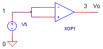
Run an AC Analysis of the SPICE file OPMODEL3_CMRR.CIR. VS drives both inputs with 1 VAC.

CIRCUIT INSIGHT Let's take a look at the common-mode error versus frequency at the input terminals. You can do this by plotting the voltage across EOS or V(1)-V(XOP.9). For a clearer view, change the Y-Axis to a Log Scale. At low frequencies, the error due to Vcm should be small. How small? We predict it to be Vcm/CMRR = 1 V / 100000 = 10 uV. Essentially, the frequency curve you're seeing represents 1/CMRR.
What happens above the corner frequency fz = 1000 Hz. Yes, the CMRR begins to lose its effectiveness and the error grows with increasing frequency.
THE REAL CMR
The CMR behavior developed here is somewhat oversimplified in a number of ways. The actual error in a real op amp results from the imbalances in the transistors and resistors of the input stage. The actual CMR can be very non-linear, especially as Vcm approaches the extremes of the common-mode range. The frequency response may be a bit more complex than a single zero. And finally, the polarity of EOS may be either positive or negative. All that said, accounting for its behavior (worst case) in your model helps you anticipate and avoid some unexpected errors in your final design.
THE EFFECTS OF CMR
CIRCUIT INSIGHT To see the effect of CMR, wire up the op amp as a unity gain, non-inverting amplifier. Drive the input with a large common-mode voltage like 10V step function. Then, run a Transient Analysis and plot 10-V(3) to see how close to 10V the output actually comes. It should be off the mark by a few hundred μV! Why? While some error is due to the finite open-loop gain of the op amp, the other is due to the common-mode error voltage. To see the effect from CMR, turn OFF the common-mode error voltage by setting EOS to a gain of 0.
EOS 1 9 POLY(1) 30 100 0 0
Now run another simulation without the effects of CMR. How much has the output changed? This change is the due to the CMR error.
What about an op amp wired up as a unity gain inverting amplifier? Drive the input with a large common-mode voltage like 10V step function and plot -10-V(3). What is the effect of turning EOS ON and OFF? You should see no effect! Why? The inverting amplifier operates with its inputs at ground - there's no voltage at Vcm to induce a CMR error!
SIMULATION NOTES
For a description of all op amp models, see
Op Amp Models.
For a quick review of subcircuits, check out
Why Use Subcircuits?
Get a crash course on SPICE simulation at
SPICE Basics.
A handy reference is available at SPICE
Command Summary.
This op amp model can be used for many of the op amp
circuits available from the Circuit
Collection page.
SPICE FILES
Download the file or copy this netlist into a text file with the *.cir extension.
OPAMP3_CMR.CIR - OPAMP MODEL W/ CMR
*
* POWER SUPPLIES
VCC	10	0	DC	+15V
VEE	11	0	DC	-15V
*
* SIGNAL SOURCE
VS	1	0	AC 1
*
XOP	1 1 3  10 11	OPAMP3
RL	3	0	10MEG
*
*
* OPAMP MACRO MODEL (INTERMEDIATE LEVEL WITH CMR)
*
*                IN+ IN- OUT  VCC  VEE
.SUBCKT OPAMP3   1   2   81   101   102
* CMR INPUT
RCM1	1	105	1000MEG
RCM2	2	105	1000MEG
EOS	1 9	POLY(1) 30 100	  0 1
*
Q1	5 9	7	NPN
Q2	6 2	8	NPN
RC1	101	5	95.49
RC2	101	6	95.49
RE1	7	4	43.79
RE2	8	4	43.79
I1	4	102	0.001
*
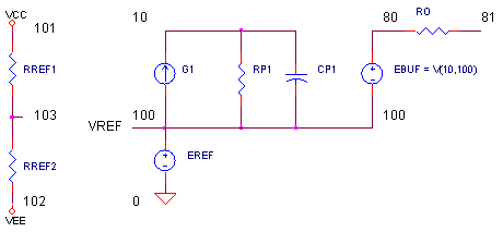
* OPEN-LOOP GAIN, FIRST POLE AND SLEW RATE
G1	100 10	6 5 0.0104719
RP1	10	100	9.549MEG
CP1	10	100	0.0016667UF
*
* OUTPUT STAGE
EOUT	80 100	10 100	1
RO	80	81	100
*
* CMR DC AND 1ST POLE
GCM	100 30	105 100 1E-11
RCM	30	31	1MEG
LCM	31	100	159
*
* INTERNAL REFERENCE
RREF1	101	103	100K
RREF2	103	102	100K
EREF	100 0	103 0 1
R100	100	0	1MEG
*
.model NPN  NPN(BF=50000)
*
.ENDS
*
* ANALYSIS
.AC 	DEC 	5 1 100MEG
*
* VIEW RESULTS
.PRINT	AC 	V(1)
.PROBE
.END
© 2004 eCircuit Center