The Miller Effect
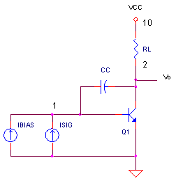
CIRCUIT
GAIN_STAGE_W_MILLER.CIR Download the SPICE file
Whether you're trying to understand an audio amplifier or the inside of an op amp, the Miller effect is key to predicting its frequency response. Typically there's a low-pass filter (pole) in the voltage gain stage created by RIN of the transistor and a feedback capacitor CC. But, the low pass cutoff is not simply determined by RIN and CC. The Miller effect creates an effective capacitance across RIN that's looks like CC scaled by the amplifier's voltage gain.
The Miller effect is especially handy when you're trying to produce a low-pass filter on an IC op amp with a relatively low frequency cut-off. Just one problem - large capacitors are difficult to make because they eat up so much real estate. The solution - make a small capacitor and then scale up its behavior using the Miller effect. Let's design an amplifier and predict its frequency response based on the Miller Effect.
EQUIVALENT CIRCUIT
Here's a simplified version of the circuit above.
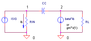
Miller said that you can approximate the input capacitance by replacing CC with a different capacitance CM across the RIN. How big is CM? It's multiplied by the voltage gain (Av = gm · RL) of the amplifier.
CM = CC · (1+Av)
How does this work? Well, we know that forcing a voltage across a capacitor causes a current to flow. How much? It depends on its capacitance: I = CC · ΔV/Δt. However, in this circuit, the voltage gain at RL causes a much larger ΔV across CC - causing an even larger current to flow through CC. Therefore, it looks like a much larger capacitance from VIN's point of view!
► Example Calculation
Suppose we've got an NPN transistor with β = 100 biased at Ic = 1 mA with CC = 30 pF. The input resistance is calculated as
RIN = β / (Ic / 26 mV) = 2.6 kΩ
The transconductance gm = ic / vin becomes
gm = Ic / VT = Ic / 26 mV = 0.0385 A / V
The voltage gain Av = V(2) / V(1) is calculated as
Av = gm · RL = 192.3 V/V
The transimpedance gain is the output voltage versus input current
Kt = β · RL = 500,000 V/A
The last two pieces of this puzzle is the input capacitance and fc of the low pass filter.
CM = CC · (1+Av) = 5770 pF
fc = 1/(2 π RIN CM) = 10.6 kHz
Cool! The Miller effect multiplies CC from a humble 30 pF to a whopping 5770 pF.
TEST CIRCUIT
Let's check out the numbers calculated in the example with a simulation. First, create a simple transistor model with β = 100.
.model QNPN NPN(BF=100)
Next we'll drive the base with two current sources: one to bias the
collector at 1 mA (IBIAS = 10 uA DC ) and another for the signal (ISIG =
1 uA peak sinewave at 100 Hz). This 100 Hz should be a low enough frequency below
before CC takes effect. At the collector we've got a 5 kΩ
resistor and a 15V supply. With Ic = 1mA, this places the collector
at Vc = 15V - 1mA·5kΩ
= 10V.
CIRCUIT INSIGHT Run a Transient Analysis and plot the input voltage V(1). What is the expected voltage here? V(1) = ISIG · RIN = 1uA peak · 2600 = 2.6 mV peak. Is this the voltage at V(1)? Next, open another plot window and add the output voltage V(2). We expect to see V(2) = ISIG · β · RL = 1uA peak · 100 · 5000Ω = 0.5 V peak. The output should be inverted of course. Okay, so what's our measured voltage gain? Av = 0.5V / 2.6mV = 192.6 V/V as calculated above!
Okay, let's see the Miller effect in action. Run an AC Analysis and plot the output V(2). The output is at 0.5V peak as calculated above. But, where is the cutoff frequency? With the output of 0.5 V peak at low frequencies, check where the magnitude falls to 0.5V * 0.707 = 0.35 V. Does your cutoff fall close to the calculated 10.6 kHz? Awesome dude - your little 30 pF capacitor acts like a 5770 pF cap around RIN (with a little help from the circuit's voltage gain.)
To see your more of the transistor in action, you can plot the following characteristics:
Current
Gain beta = I(RL) / I(ISIG)
Transconductance gm = I(RL) / V(1)
Voltage Gain Av = V(2) / V(1)
Transimpedance Gain Kt = V(2) / I(ISIG)
Are they close to the values we calculated above?
HANDS-ON DESIGN Let's play with this circuit a bit. Try lowering the cutoff frequency by increasing CC from 30 pF to something like 300 pF and plot V(2). Does fc drop by the approximately same factor as CC's increase? Now, reduce the Miller effect by decreasing RL from 5000 to 500 effectively dropping the voltage gain. What happen to the CM and fc now?
SPICE FILE
Download the file or copy this netlist into a text file with the *.cir extension.
GAIN_STAGE_W_MILLER.CIR
*
IBIAS	0	1	DC	10UA
ISIG	0	1	AC	1UA	SIN(0 1UA 100HZ)
*
* GAIN STAGE / MILLER EFFECT
Q1	2 1	0	QNPN
CC	1	2	30PF
RL	2	10	5000
VCC	10	0	DC	+15V
*
.model	QNPN	NPN(BF=100)
*
* ANALYSIS
*
.TRAN	0.1US 10MS
.AC DEC 5 10 100MEG
.PROBE
.END
© 2007 eCircuit Center