Transmission Line Terminations
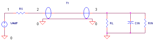
CIRCUIT
TLINE1.CIR Download the SPICE file
Drive a high-speed signal (digital data or video) into one end of a long coax cable and you might be surprised - at both ends of the cable! Over long distances, electric signals act more like traveling waves than instantaneous changing signals. What kind of effects can result? In the classic analogy, a ripple travels smoothly in a pool because one volume of water has the same "impedance" as the next. However, a wall or human body, presenting a very different impedance, reflects the wave in the opposite direction.
In video signals, reflections occur in a similar manner at mismatched impedances creating distortions and ghosting. Digital signals may show slow rise times or spurious transitions through the logic threshold region. What can you do about it? Matching the electrical impedance of the cable at one or both ends can reduce reflections dramatically. But before you make a decision, you need to understand the pros and cons of each option.
LINE IMPEDANCE AND REFLECTIONS
For short rise times or high frequencies a transmission line (coax cable, twisted ribbon cable pair, PCB trace over a ground plane) displays a characteristic impedance (50 - 300 Ω), depending on its materials and physical dimensions. A signal traveling down a line will be transferred without reflection if the load impedance RL matches the line impedance Z0. If not, part of the wave is reflected. How much? A simple equation predicts the ratio of reflected Vr to incident Vi amplitude
Vr / Vi = ( RL - Z0 ) / ( RL + Z0 )
Three cases show the range of values for the reflected wave
Matched Load: RL = Z0 Vr / Vi = 0 No reflection.
Open Load: RL = ∞ Vr / Vi = +1 Full reflection, same polarity.
Shorted Load: RL = 0 Vr / Vi = -1 Full reflection, inverted polarity.
UNTERMINATED CABLE
Suppose you need to drive a video or high speed digital signal to a remote instrument or monitor over a 75 ohm cable. In the circuit above, amplifier VAMP represents your line driver with a source impedance RS = 5 Ω. At the other end of the cable (5 meters) is the input impedance of the line receiver, RIN = 10k Ω and CIN = 10 pF. The terminating resistor RL is essentially not in the circuit RL = 1MEG. Basically, the load looks like an open circuit compared to the 75 ohm cable.
CIRCUIT INSIGHT Simulate the SPICE file TLINE1.CIR. Amplifier VAMP produces a 1V voltage step with a short rise time. Plot V(2) and V(3), the voltages at both ends of the cable. How long does the rising edge take to reach the end of the cable? You should see a delay of about 20 ns.
What happened to the step voltage at the load end? What caused these unspeakable horrors to the step waveform? According to the equations above, the cause was a full positive reflection at the load! Together, the 1V (approx.) reflected wave adds to the 1V incident wave resulting in the near 2V level at the load end. Now, what happens to the reflected wave as it returns to the source VAMP. This returning wave essentially sees a short (RS = 5 Ω) and produces an inverted reflection that travels back to the load. The cycle repeats to create ringing on the line.
LOAD TERMINATION
Terminating the line correctly can remedy the situation. To make the load appear like just another segment on the transmission line, place a resistor, RL = 75 Ω, at the end of the cable. The step function should be transferred to the load without reflection.
HANDS-ON DESIGN Change RL to 75 Ω and rerun TLINE1.CIR. Check out V(2) and V(3). Is the step function preserved?
All is well (almost). You may have noticed a little blip at V(3). What causes this? Actually, the 75 Ω terminator is not really 75 Ω. There's a capacitor CIN = 10 pF shunting RL = 75 Ω causing it to be less than its expected value for short rise times. To see a blipless waveform, temporarily remove CIN by placing a * at the beginning of the CIN line. Rerun the simulation. Has the blip disappeared? Return CIN into the circuit by removing the *.
Load terminations come with a price. Plot the required amplifier current by adding trace I(RS) in a separate plot window. Notice the amplifier needs to source 12.5 mA of current for the 1 V step function!
SOURCE TERMINATION
As another termination option, place a 75 Ω resistor in series with the amplifier and leave RL open. If your amplifier's output impedance is 5 Ω, insert a 70 Ω resistor for a 75 Ω total. The waveforms get a little more interesting for a source match. But the bottom line is the same, the waveform is preserved at the load end.
HANDS-ON DESIGN Modify TLINE1.CIR for RS = 75 Ω and RL = 1MEG. Rerun a simulation and check out V(2) and V(3). Notice that the initial voltage at V(2) is 0.5 V! That's because RS = 75 Ω and Z0 = 75 Ω act like a voltage divider sending only 0.5 V down the line. But, there's help waiting at the load end. Because the load end is open, a full reflected wave occurs and the 0.5 V incident wave adds to the 0.5 V reflected wave for the total 1.0 V level. The 0.5V reflected wave travels back to the matched source getting absorbed without further reflections.
Here's an advantage of the series termination at the source end. Look at the source current by plotting I(RS) in a separate plot. The amplifier needs to supply current only during time the initial wave travels to the load and back. A disadvantage may occur if the cable is not exactly 75 Ω due to manufacturers tolerance. Change the line impedance of T1 to Z0 = 70 or 80 Ω and test drive the circuit. The signal may require a few additional reflections before settling down.
SOURCE AND LOAD TERMINATION
One of the most effective options is matching the impedance at both the source and load ends. This configuration helps minimize distortions at the load even when the terminations do not exactly match the cable impedance. However, a DC voltage divider is formed by RS = 75 Ω and RL = 75 Ω. To compensate for this reduction in signal, boost the amplifier's signal up from 1 to 2 V.
HANDS-ON DESIGN Modify TLINE1.CIR for RS = RL = Z0 = 75 Ω. Remember to crank up the drive voltage by changing VAMP's voltages to 2V. Run a simulation and check out V(2) and V(3). Does the 1V step arrive at the load as expected?
Simulate the cable manufacturer's variations by changing T1's impedance to Z0 = 70 or 80 Ω. What is the impact on the waveform at V(3)? It should be minimal.
SIMULATION NOTES
Transmission lines are defined by two parameters: characteristic impedance Z0 and delay time TD. What is the delay time? This tells you how long it takes a step voltage to travel from one end of the cable to the other. The time delay is easily determined by the cable speed and cable length. In the circuit above, the 5 meter cable is specified as having a speed of 85% compared to the speed of light. The time delay is calculated as
Time = Length / Speed = 5 m / (0.85 ∙ 300e6 m/s) = 19.6 ns.
The SPICE transmission line looks like
T1 2 0 3 0 Z0=75 TD=19.6NS
where nodes 2 0 and 3 0 are the connections at either end of this bidirectional device.
SPICE FILE
Download the file or copy this netlist into a text file with the *.cir extention.
TLINE1.CIR - TERMINATED TRANSMISSION LINE
*
* AMPLIFIER, SIGNAL RISE TIME = 10NS
VAMP	1	0	AC	1	PWL(0NS 0V  10NS 1V  300NS 1V)
*
RS	1	2	5
*
* 75 OHM COAX, 5 METERS LONG, RELATIVE VELOCITY 85%
* TD = 5 METERS / ( 0.85 * 300MEG METERS/SEC) ) = 19.6N SEC
T1	2 0	3 0	Z0=75	TD=19.6NS
*
RL	3	0	1MEG
*
* INPUT Z OF RECEIVER
RIN	3	0	10K
CIN	3	0	10PF
*
* ANALYSIS
.TRAN	1NS	300NS
*
* VIEW RESULTS
.PRINT	TRAN	V(2) V(3)
.PROBE
.END
© 2002 eCircuit Center