SMPS - VOLTAGE MODE CONTROL
CIRCUIT

BUCK_VM1.CIR Download the SPICE file
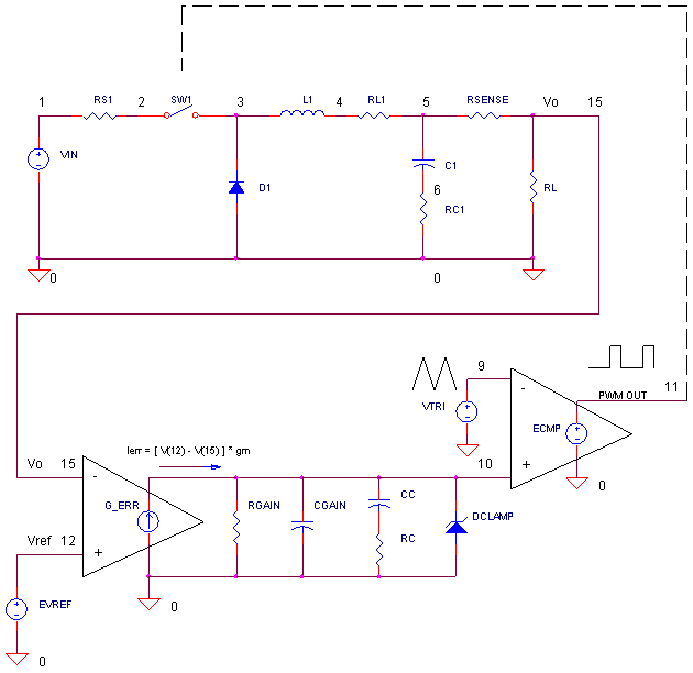
In a previous topic, we checked out the basic topology of the Buck Converter. Fine for learning, but no use in a real application! Why? Varying input voltage and load conditions cause the output voltage to change! How do you maintain a precise Vo? Placing the Buck inside of a control loop holds Vo at a rock solid level. A few simulation challenges pop up here. How do you create SPICE models for components like Pulse-Width-Modulators (PWMs) and comparators? And how can you model the error amplifier that's inside your typical Buck Controller IC.
CLOSING THE LOOP
What does closing the loop do for you? A closed-loop control system automatically maintains a precise output voltage regardless of varying input and load conditions! How? The main mission of the control loop is this:
► Adjust the duty cycle of the PWM to bring the output voltage Vo equal to
the reference voltage Vref.
Why call it voltage mode? Varying the duty cycle essentially adjusts the input voltage drive to the Buck's LC components which directly effects Vo. Now we'll look at control components we wrap around this basic topology. (The basic Buck was covered in a previous topic, the Buck Converter.)
ERROR AMPLIFIER
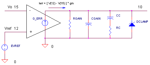
An essential part of automatic control is measuring how close Vo is to Vref.

This measurement of error is simply their difference, Ierr = Vref - Vo. This error current then drives the PWM!
If Vo < Vref, then Ierr is positive - increase V(10) and the PWM duty cycle.
If Vo > Vref, then Ierr is negative - decrease V(10) and the PWM duty cycle.
If Vo ~ Vref, then Ierr is close to zero - maintain V(10) and the PWM duty cycle
In the SPICE file, G_ERR 0 10 12 5 0.002 generates a current (node 10) equal to Vo (node 15) subtracted from Vref (node 5), or
Ierr = ( Vref - Vo ) ∙ 0.002
where 0.002 is the transconductance gain (gm = Iout/Vin). To convert Ierr into a voltage, RGAIN = 500 kΩ is placed across G_ERR for an error voltage of
Verr = ( Vref - Vo ) ∙ 0.002 ∙ 500 k
= (Vref - Vo ) ∙ 1000
The overall voltage gain of the error amplifier becomes 1000 V/V. Capacitor CGAIN models the bandwidth limit of the error amplifier.
What's RC and CC's role? They reduce the gain at high frequencies. Why? To keep the supply from wild ringing or oscillations (a later topic). DCLAMP, as the name suggests, clamps Verr to an approximate range 0 to 5 V.
PWM
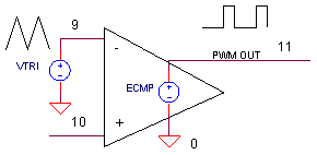
How do you assemble a PWM? Just two simple components are needed: a triangle wave and a comparator.

As node 10 changes from 0 to 5 V, the output V(11) changes from 0% to 100% duty cycle. SPICE isn't equipped with a triangular wave, per se. However, a pulse generator ( Tperiod = 10 us ) with long rise and fall times ( 4.9 us ) creates a suitable triangular wave.
VTRI 9 0 PULSE( {v1} {v2} {tdelay} {trise} {tfall} {width} {period} )
PULSE( 0V 5V 0US 4.9US 4.9US 0.1US 10US )
To model the comparator, we put the TABLE function into action.
ECMP 11 0 TABLE {V(10,9)} = (-5MV 0V) (5MV, 5V)
This statement defines points (input,output) of a Piece-Wise-Linear transfer function describing the output V(11) versus input V(10)-V(9). If V(10)-V(9) less -5 mV, then the output remains fixed at 0 V. If V(10)-V(9) is between -5V and +5 mV, then the output is linearly interpolated between 0 and 5V. And if V(10)-V(9) is greater +5 mV, then the output remains fixed at 5 V. In a nutshell, the table implements a comparator function having an internal gain of Av = (5V-0V)/(5mV-(-5mV)) and output saturation levels of 0 and 5 V.
THE ULTIMATE TEST
Let's see if automatic control fulfils its promise. What's the ultimate test for a supply? Vary the input voltage and load levels. Can the Buck hold Vo to a steady 5V?
CIRCUIT INSIGHT Run a SPICE simulation of the file BUCK_VM1.CIR. The simulation runs for 2000 us. Plot the reference voltage V(12), the output voltage V(15). Open another plot window and plot the input voltage V(1) and output current I(RSENSE). (Notice RSENSE, a small valued resistor, is tossed in the circuit only to sense output current.)
Vref at V(12) ramps up from 0V to 5V, then holds steady at 5 V. How well does the output V(15)
follow
V(12)? Hey looking good! Maybe, a little overshoot and ringing, but
Vo rises to 5V in a couple milliseconds. Okay no more Mr. nice guy. Let's drop the
input battery voltage VS from 12 to 10V, 9V or lower. Does the output hold
to 5V? At what point are the conditions too severe?
Return VS to 12V. Now increase the load by dropping RL from 5 to 2.5 Ω or lower. How well does Vo hold up?
CONTROL CLOSE-UP
To see the control loop in action, open an additional plot window and plot the error voltage V(10) and the PWM output V(11).
CIRCUIT INSIGHT Check out the control loop as it varies the duty cycle attempting to bring Vo close to Vref. Shorten the analysis time from 2000 to 200 μs. The PWM duty cycle at V(11) should be directly proportional to the error voltage at V(10). Raise or lower the input voltage VS to values like 24 or 8V. How does this effect the overall duty cycle? A greater VS should mean a smaller duty cycle.
THE PULSED LOAD TEST
Another useful measure of a supply is its response to a pulsed load. To accomplish this, create a pulsed current source. (Simply remove the comment character "*" before the ILOAD statement already in the file.)
ILOAD 15 0 PWL(0US 0A 1000US 0A 1001US 1A 1500US 1A 1501US 0A 2000US 0A)
ILoad sinks an additional 1 A from the load between 1000 and 1500 us.
CIRCUIT INSIGHT
Rerun the SPICE file. Check out the total load current
I(RSENSE) and the output
voltage V(15). How does the control loop respond to the
additional demand?
VOLTAGE GAIN
Need a voltage higher than 5V? Add voltage gain by installing a resistor divider at the output.
R2 15 16 1K
R1 16 0 1K
Now, feed the divider tap back to the error amplifier. (Change node 15 to 16 in the G_ERR statement.)
G_ERR 0 10 12 16 0.002
Your output voltage will now be Vo = 5V ∙ (R2 +R1)/R1 = 5V ∙ 2 = 10 V. Why? The control loop now brings the divider tap V(16) to Vref = 5V. But, the voltage across the divider, or Vo, must be bigger by an amount defined by the divider equation.
HANDS-ON DESIGN Modify the file as shown in the statements above and rerun the SPICE file. Does the R1,R2 voltage divider force the output to 10V ? Change the divider resistors to some other ratio. Does Vo change as expected?
SIMULATION NOTES
Understand the basic operation of the
Buck Converter.
The
Buck Converter AC Model
helps you create an AC SPICE model.
Tuning a Buck Converter lets you compensate
a converter for minimum overshoot and ringing.
Find out where SMPS power gets wasted in the topic
Buck Converter Power Loss.
SPICE FILE
Download the file or copy this netlist into a text file with the *.cir extension.
BUCK_VM1.CIR - BUCK CONVERTER - VOLTAGE MODE CONTROL
*
* INPUT VOLTAGE
VS	1	0	DC	12
RS	1	2	0.1
*
* BASIC BUCK TOPOLOGY
S1	2 3	11 0 	SW
D1	0	3	DSCH
L1	3	4	50UH
RL1 4	5	0.01
CL	5	6	200UF
R_ESR	6	0	0.1
* MEASURE TOTAL CURRENT OUT W/ RSENSE
RSENSE	5	15	0.01
*
* LOAD
RL	15	0	5
* PULSED LOAD
*ILOAD 15 0	PWL(0US 0A  1000US 0A   1001US 1A  1500US 1A  1501US 0A   2000US 0A)
*
* VOLTAGE MODE CONTROL
* REFERENCE VOLTAGE
VREF	12	0	PWL(0US 0V  10US 0V   201US 5V  1000US 5V)
*
* ERROR AMP AND COMPENSATION
G_ERR	0 10	12 15	0.002
RGAIN	10	0	500K
CGAIN	10	0	10PF
CC	10	7	0.2UF
RC	7	0	2000
DCLAMP	0	10	DZ45
*
* TRIANGLE WAVE FOR PWM
* (PULSE SOURCE WITH LONG RISE/FALL TIMES)
VTRI	9	0	PULSE(0V 5V 0 4.9US 4.9US 0.1US 10US)
R9	9	0	1MEG
*
* PWM COMPARATOR
ECMP	11	0	TABLE {V(10,9)} = (-5MV 0V) (5MV, 5V)
R11	11	0	1MEG
*
*
.MODEL	SW	VSWITCH(VON=5V VOFF=0V RON=0.1 ROFF=100K)
.model	DZ45	D( BV=4.5 )
.MODEL DSCH D( IS=0.0002 RS=0.05 CJO=5e-10  )
*
* ANALYSIS
.OPTIONS ABSTOL=1M RELTOL=1M ITL5=0
.TRAN 	1US  	2000US
*
* VIEW RESULTS
.PRINT	TRAN	V(1) V(15)
.PROBE
.END
© 2006 eCircuit Center