Pulse Width Modulation
CIRCUIT
PWM.CIR Download the SPICE file
One of the biggest problems with delivering power to a load (motor, heater, etc.) is in the power lost and heat dissipated in the output stage. And given the industry's boom in battery-powered portable devices, power lost means a shorter battery life and heat dissipated implies larger more expensive components (power semiconductors and heat sinks).
How can you reduce this wasted power? One clever method is a technique called Pulse Width Modulation (PWM). A conventional linear output stage applies a continuous voltage to a load. This can waste plenty of power (more below). On the other hand, PWM applies a pulse train of fixed amplitude and frequency, only the width is varied in proportion to an input voltage. The end result is that the average voltage at the load is the same as the input voltage; but with less wasted power in the output stage. How much advantage does PWM provide? After building a PWM system, we'll face it off against a linear output stage. The champion will be the most efficient power delivery system.
When should you use PWM? If the pulse period is much shorter than the time-constant of the load, then PWM has a potential application. The time-constants are defined, for example, by the thermal mass of a resistive heater or the mechanical inertia of a motor. And it's the long time-constants that average the pulses to a desired value set by the PWM's input voltage.
PULSE WIDTH MODULATOR
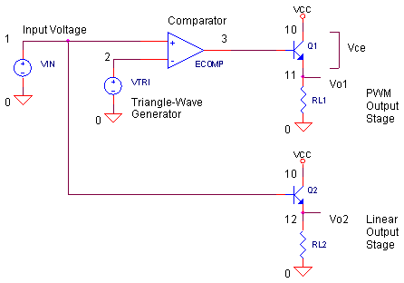
How do you generate a pulse train whose width is proportional to the input voltage? It's easier than you may think. Just two system components are needed: a triangle wave generator and a comparator. To demonstrate the operation of the PWM, let's build it with high level SPICE components. Voltage source VTRI generates the triangle waveform (10kHz) and ECOMP mimics the comparator function. The operation is simple; when the input voltage VIN is less than the triangle wave, the output of the PWM is low (0V). When VIN is greater than the triangle wave, the output is high (10V). It's a simple and elegant solution to a seemingly tough design challenge.
CIRCUIT INSIGHT Simulate the SPICE file PWM.CIR. The triangle generator output ramps between 0V and 10V. Source VIN applies a sinewave (± 4V, centered around 5V, 500 Hz) to the input of the PWM. Plot the input voltage V(1) and the PWM output V(3). Can you see the pulse width vary in proportion to the input voltage? Add trace V(2) to see the triangle wave relative to the input V(1). If you want a better view of the operation, shorten the length of the transient analysis from 2000 to 500 us.
INPUT RANGE
HANDS-ON DESIGN You can design a PWM for any input range by adjusting the triangle wave swing. Choose a new input voltage range. Then, adjust the triangle wave output to include the new input range. (Example: For an input range of ± 5 V, adjust the triangle wave generator for a -5 V to +5 V output swing. The new device statements would look like VIN 1 0 SIN(0V 5V 500HZ) and VTRI 2 0 PULSE(-5V 5V...) Return the length of the transient analysis back to 2000 us. Test drive your new PWM and view the input V(1) and output V(3).
OUTPUT STAGE POWER
A simple emitter follower Q1 serves as the PWM's output stage. This transistor is driven into one of two states: fully ON or fully OFF. And therein lies the virtue of the PWM. In either of these states, the transistor power is LOW. Why? You can calculate Q1's power by
PQ1 = VCE x ILOAD
For both states, the power for Q1 appears below.
| Q1 state | Q1 power | |
| Full ON | PQ1 = VCE (LO) x ILOAD (HI) = LO Power | |
| Full OFF | PQ1 = VCE (HI) x ILOAD (LO) = LO Power |
CIRCUIT ANALYSIS Set VIN to a 5V DC level and return the triangle wave to its original 0 to 10V swing (VIN 1 0 SIN(5V 0V 500HZ) and VTRI 2 0 PULSE(0V 10V...) Run a simulation and plot the power lost to Q1 by adding trace
I(RL1)*(V(10)-V(11))
(For TopSpice users, display Q1's power by uncommenting the statement #CALC PQ1=I(RL1)*(V(10)-V(11))before running a simulation, then, adding trace PQ1.) What you should see is the instantaneous power lost to Q1. Three interesting points leap off the display: 1) The power is 0W when the transistor is OFF, 2) The power is only about 0.4 W when the transistor is ON, and 3) spikes occur when the transistor switches ON or OFF. What's the bottom line for Q1's power dissipation? Taking the average power, Q1 only consumes about 0.2 W!
PWM VS. LINEAR OUTPUT STAGE
Now, let's bring in the linear output stage Q2 to check its efficiency versus the PWM output stage. As you may have picked up already, the linear stage gulps plenty of power. The only question is: how much? Q2 is driven directly from VIN. An emitter follower is a typical output stage for an audio or servo amplifier. The worst case is when the output is half the supply voltage. For example, for a 10V supply, an output voltage of 5V across RL2 leaves the other 5V across Q2. And the equation PQ2 = VCE x ILOAD tells us there's some serious power to be dissipated in Q2.
CIRCUIT ANALYSIS Plot the power lost to Q2 by adding trace
I(RL2)*(V(10)-V(12))
(For TopSpice users, display Q2's power by uncommenting the statement #CALC PQ2=I(RL2)*(V(10)-V(12))before running a simulation, then, adding trace PQ2.) The linear output stage dissipates a jaw-dropping 1.2 W! On the other hand, the PWM output stage (our efficiency champion) delivers the same average power to the load while only consuming 0.2 W!
SIMULATION NOTES
Two simple tricks make simulating the PWM system easy. First, the triangle waveform is generated by a PULSE source VTRI. Typically, the pulse source looks like a digital waveform. However, by specifying atypically long rise and fall times, the pulse train looks very much like a triangle wave.
Second, the comparator is simulated by a nifty method of using an input/output TABLE to specify the transfer function of a controlled source. The Voltage Controlled Voltage Source (VCVS) defined by
ECOMP 3 0 TABLE {V(1,2)} = (-1MV 0V) (1MVS, 10V)
takes the input at V(1,2) and produces an output at V(3,0) according to the table below
| input V(1,2) | output V(3,0) | |
| ≤ -1mV | 0V | |
| -1mV < V(1,2) < +1mV |
A Piece-Wise-Linear transfer function defined by a line between (input,output) points (-1mV, 0V) and (+1mV, +10V). |
|
| ≥ +1mV | +10V |
SPICE FILE
Download the file or copy this netlist into a text file with the *.cir extention.
PWM.CIR - PULSE WIDTH MODULATION
*
* INPUT VOLTAGE
VIN	1	0	SIN(5V 4V 500HZ)    ;SIN(Offset Peak Freaquency)
RIN	1	0	1K
*
* 10KHZ TRIANGLE WAVE
* (GENERATED USING PULSE SOURCE WITH LONG RISE/FALL TIMES)
VTRI	2	0	PULSE(0V 10V 0 49US 49US 1US 100US)
RTRI	2	0	1MEG
*
* COMPARATOR, INPUT = V(1,2)
* FOR V(1,2) < -1mV, OUTPUT = 0V
* FOR V(1,2) > +1mV, OUTPUT = 10V
ECOMP	3	0	TABLE {V(1,2)} = (-1MV 0V) (1MV, 10V)
RCOMP	3	0	1MEG
*
* PWM OUTPUT STAGE
VCC	10	0	DC 10V
Q1	10	3 11	QNOM
RL1	11	0	20
*
* LINEAR OUTPUT STAGE
Q2	10	1 12	QNOM
RL2	12	0	20
*
.model	QNOM	NPN
*
* ANALYSIS
.TRAN 	5US  	2000US
* VIEW RESULTS
.PRINT	TRAN	V(1) V(3)
* TOPSPICE CALCULATIONS
*#CALC  PQ1=I(RL1)*(V(10)-V(11))
*#CALC  PQ2=I(RL2)*(V(10)-V(12))
.PROBE
.END
© 2002 eCircuit Center