Push-Pull Output Stage
CIRCUIT
PUSHPULL.CIR Download the SPICE file
Whether you're delivering power to a loudspeaker or a servo amplifier,
the push-pull output stage (Class B) can be a good choice for the job. One
advantage is that there's no power dissipated in the output transistors when
there is no signal present. (The Class A stage requires significant bias -
and dissapates lots of heat - even with no input signal.) One disadvantage
of the push-pull is the distortion of the signal near 0V. Distortion can be
a dirty word, especially to audiophiles. However, there are ways to reduce
it. Let's see how much of the distortion we can bring down using some simple
techniques.
PUSH-PULL OUTPUT STAGE
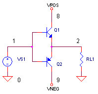
This circuit is formally called the Complementary Symmetrical Push-Pull output stage. Taking the stuffiness out of the terms, the name says that 1) the stage has an NPN and a PNP device. 2) the NPN and PNP circuits look the same. 3) the stage can both source and sink current. Because the circuit is really only a couple of emitter followers driving the same load, the operation is simple; Q1 conducts on positive swings; Q2 conducts on negative swings.
CIRCUIT INSIGHT Run a simulation of PUSHPULL.CIR. A 5V peak sinewave at 10 kHz is applied to the input. Plot the input V(1) and output V(2) voltages. Take look at that "sinewave" output - its got ugly written all over it! Why? Remember the output stages are simple emitter followers. And it takes about 0.7 V to turn ON a transistor. This means Q1's emitter won't begin to move positive until the input reaches +0.7 V. Likewise, Q2's emitter won't budge negative until the input goes below -0.7 V. In effect, any input signal between +/-0.7 V has entered the "dead-zone" leaving the output stuck at 0V. Another undesirable effect is that the output falls short of the 5V peak by about 0.7 V.
HOW MUCH DISTORTION?
SPICE provides a convenient way to determine the Total Harmonic Distortion (THD) of your output signal. By including the command
.FOUR 10KHZ V(2)
SPICE calculates the Fourier Series of the voltage V(2) using 10kHz as the fundamental frequency. If your signal is a pure sinewave with no distortion, the Fourier Series will show a large component V1 at the fundamental 10kHz with no components, V2, V3, V4,..., at harmonic frequencies of 20kHz, 30kHz, 40kHz,.... On the other hand, a distorted wave shows significant components at the harmonics. The THD is easily calculated as
![]()
The PUSHPULL.CIR file includes the .FOUR statement as shown above. To view the results, open the output file (*.OUT) generated by the simulation. The table should show the fundamental and harmonic frequencies and the energy present at each frequency. What is peculiar about the result? Notice that only the odd harmonics (10kHz, 30kHz, 50kHz,...) have significant values. This is typical of waveforms that are distorted symmetrically around 0 V. Finally, what is the THD of the output signal? SPICE also calculates this for you. A THD of 10% or so would not be music to your ears when heard through a loud speaker.
DIODE BIAS
What we need is a way to make up for the 0.7 V loss of the emitter followers. So we ask ourselves: what component has an ON voltage close to a VBE drop? The answer is the PN juntion diode. A schematic showing two diodes cleaning up the dead-zone appears below.
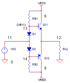
Its a simple but effective solution to the distortion problem. As you can
see, diode D1 adds about 0.7 V to the input signal, roughly the same amount
dropped, -0.7 V, by the NPN emmiter follower Q11. The net effect is that the
VD1 and VBE cancel one another, preserving (approximately) the input level.
Diode D2 does the same thing for Q12, only in the opposite polarity.
So how much do you bias into D1? RB1 controls D1's current. A larger current
(smaller RB1) means a larger diode voltage and consequently a greater Vbe
with no input signal. This increased bias should reduce distortion even
further. But, be careful not to make RB1 too small. The resulting higher
diode current - and higher diode voltage - starts to forward bias Q1 causing
collector current to flow, even with no input signal. At this point, the
transistor has moved into a Class AB bias. This may be okay as long as you
account for the extra power dissipation in Q1. (A further danger of too much
bias is the transistor going into thermal runaway as it heats up.)
At the other extreme, reducing RB1 may limit the maximum output swing. Keep
in mind, RB1 has 2 jobs: 1) to deliver base current into Q11 and 2) to provide bias
current into D1. You can calculate the current through RB1 by IRB1 = (VPOS -
VB11) / RB1. The equation tells you that IRB1 gets smaller as VB11 increases. A
point is reached where there's not enough IRB1 to supply both D1 and Q11. As
the input increases, diode D1 eventually shuts OFF leaving the output flat for
the remainder of the voltage peak.
CIRCUIT INSIGHT
Run a simulation of PUSHPULL.CIR. Plot the output
voltage V(12) of the improved stage. What's the first thing you notice about
the sinewave output? The shape has improved dramatically! Not only that, but
the output peak almost reaches the full 5V. So how much has the THD
improved? Perform a Fourier Analysis on the output V(12) by changing the
analysis statement to look like .FOUR
10KHZ V(2) V(12). Hopefully, we've
knocked down the THD below 2% with the simple diode bias trick.
HANDS-ON DESIGN Let's play with RB1 to try to knock down the THD some more. Lower RB1 from 10k to a value like 1k. Rerun the simulation. Did the THD come down any? On the other hand, if its low power you're after, increase RB1 to reduce the bias current in the output stage. But, how large can you make RB1 before the output goes flat near the peaks? (A solution to the flat-top syndrome may be to replace RB1 with a current source that's not dependent on VB11, or, pick a transistor with a higher Beta.)
OUTPUT STAGE IN A FEEDBACK LOOP
You've heard of the healing powers of feedback to cure circuit ailments like drifts and non-linearities. Now, let's put it to the test in our quest to clean up a distorted sinewave. Below is a push-pull stage enclosed in a feedback loop of a simple unity-gain op amp circuit.
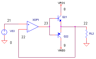
We've even removed the diode bias to put the feedback loop to a real fire test of it's curative powers. To understand the operation, remember that the op amp has one main mission in life: to make the negative input follow the positive input. And, the output will do whatever necessary in order to make it happen.
CIRCUIT INSIGHT Run a simulation and plot the input V(21) and output voltage V(22) of the output stage with feedback. Yes, we see and we believe - the input and output are almost indistinguishable! How is this possible? Take a look at the op amp's output, V(23). As expected, op amp's output compensates for the 0.7 V drop of the emitter followers. Notice how the output speeds through the "dead-zone" in order to preserve the sinewave shape at the transistor output!
Perform a Fourier Analysis on the output V(22) by changing the analysis statement to look like .FOUR 10KHZ V(2) V(12) V(22). The THD should now be squashed down somewhere below 0.1%.
FURTHER ADVENTURES There's a couple of things you can try with this circuit. First, add in the diode bias as in the previous circuit. Does the THD improve any? Second, you can add some gain to this stage by adding two feedback resistors; one from RL3 to the op amp's negative input and the other from the negative input to ground. The gain is the same as for an op amp non-inverting amplifier. Just make sure you reduce the input voltage so you won't overdrive the output stage.
SPICE FILE
Download the file or copy this netlist into a text file with the *.cir extention.
PUSHPULL.CIR - COMPLIMENTARY-SYMMETRICAL PUSH-PULL OUTPUT STAGE
*
* SUPPLY VOLTAGES
VPOS	8	0	DC	+15V
VNEG	9	0	DC	-15V
*
* PUSH-PULL TRANSISTOR OUTPUT STAGE ***************************
VS1	1	0	SIN(0V 5VPEAK 10KHZ)
*
Q1		8 1	2	QNPN
Q2		9 1	2	QPNP
RL1	2	0	100
*
* PUSH-PULL WITH DIODE BIAS ***********************************
VS2	10	0	SIN(0V 5VPEAK 10KHZ)
*
D1	13	10	DNOM
RB1	13	8	10K
Q11	8 13	12	QNPN
*
D2	10	14	DNOM
RB2	14	9	10K
Q12	9 14	12	QPNP
*
RL2	12	0	100
*
* PUSH-PULL PLACED IN OPAMP FEEDBACK LOOP *******************
VS3	20	0	SIN(0V 5VPEAK 10KHZ)
*
Q21	8 23	22	QNPN
Q22	9 23	22	QPNP
RL3	22	0	100
*
XOP1	20 22	23	OPAMP1
*
*
* DEVICE MODELS - ALL DEFAULT PARAMETERS EXCEPT BF
.model	QNPN	NPN(BF=50)
.model	QPNP	PNP(BF=50)
.model	DNOM	D()
*
OPAMP MACRO MODEL, SINGLE-POLE
* connections:      non-inverting input
*                   |   inverting input
*                   |   |   output
*                   |   |   |
.SUBCKT OPAMP1      1   2   6
* INPUT IMPEDANCE
RIN	1	2	10MEG
* GAIN BANDWIDTH PRODUCT = 10MHZ
* DC GAIN (100K) AND POLE 1 (100HZ)
EGAIN	3 0	1 2	100K
RP1	3	4	1K
CP1	4	0	1.5915UF
* OUTPUT BUFFER AND RESISTANCE
EBUFFER	5 0	4 0	1
ROUT	5	6	10
.ENDS
*
* CHECK DISTORTION WITH FOURIER SERIES ANALYSIS
.FOUR 10KHZ V(2)
*
* ANALYSIS
.TRAN	1US 200US
*
* VIEW RESULTS
.PRINT TRAN	V(2)
.PLOT	TRAN V(2)
.PROBE
.END
© 2002 eCircuit Center