Op Amp Input Offset Voltage
CIRCUIT
OP_VOFF.CIR Download the SPICE file
Build any op amp circuit, apply 0V to its input, and what do you expect at the output? Although you'd be tempted to say 0 V, there's actually an error voltage present at its output. What causes this error? You can trace the error back to a number of imbalances in the op amp's internal transistors and resistors.
To account for this in a circuit design, the net error is modeled as an input offset voltage, Voff, in series with op amp's input terminals. How will it affect your circuit?
INPUT OFFSET VOLTAGE
The input offset voltage can range from microvolts to millivolts and can be either polarity. Generally, bipolar op amps have lower offset voltages than JFET or CMOS types.
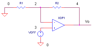
The offset voltage is modeled in series with one of the op amp input terminals. Which one? Although the net effect is the same at either input, it's much easier to analyze Voff in series with the positive (V+) input. Why? The resulting circuit with Voff at V+ looks just like the non-inverting amplifier configuration. The analysis for this circuit is a simple one.
OUTPUT ERROR
Ignoring Voff for a moment, is the circuit (shown above) an inverting or non-inverting amplifier? The answer is yes, both! With the input signal source set to 0 V ( shorted ), the inverting and non-inverting amplifiers look the same. The analysis for offset voltage is independent of the amplifier configuration. You can predict the error at the output Vo by the equation for the non-inverting amplifier
Vo_error = Voff * ( R2+R1 )/R1
What is this equation warning you about? If you have a large signal gain in your circuit, the amplifier increasees the error Voff along with the signal.
CIRCUIT INSIGHT
Run a simulation of OP_VOFF.CIR.
Voltage source VOFF
models the offset voltage, initially set to +1 mV. With R1 = 10k and R2 =
100 k, what is the error at the output V(4)? The output error gets bumped to a
whopping 11 mV as predicted by the equation above.
Choose a different gain and/or offset voltage. Run a simulation. Is the output error what you expected?
TEMPCO
But wait, there's more trouble. The input offset voltage will change ∆V (voltage drift) with a change in temperature ∆T. This error is a linear function of temperature and is defined by
Voff_TC = ∆Voff / ∆T (V/deg C)
For an with a voltage of 25 uV / deg C, what is the drift over, say ∆T = 10 deg C?
Voff = Voff_TC · ∆T
= (25 uV / deg C) · 10 deg C
= 0.25 mV
Knowing your overall error budget, you can select an op amp with a low enough offset drift to meet the target circuit performance.
INPUT BIAS CURRENT
Input offset voltage is not the only error of the op amp's input.
(See Op Amp Input Bias Currents
)
SPICE FILE
Download the file or copy this netlist into a text file with the *.cir extention.
OP_VOFF.CIR - OPAMP OFFSET VOLTAGE
*
* AMPLIFIER CIRCUIT
*
R1	0	2	10K
R2	2	4	100K
XOP1	3 2	4	OPAMP1	;V+ V- VOUT
*
* OPAMP INPUT OFFSET VOLTAGE
VOFF	3	0	DC	1MV
*
*
* OPAMP MACRO MODEL, SINGLE-POLE
* connections:      non-inverting input
*                   |   inverting input
*                   |   |   output
*                   |   |   |
.SUBCKT OPAMP1      1   2   6
* INPUT IMPEDANCE
RIN	1	2	10MEG
* GAIN BW PRODUCT = 10MHZ
* DC GAIN (100K) AND POLE 1 (100HZ)
EGAIN	3 0	1 2	100K
RP1	3	4	1K
CP1	4	0	1.5915UF
* OUTPUT BUFFER AND RESISTANCE
EBUFFER	5 0	4 0	1
ROUT	5	6	10
.ENDS
*
* ANALYSIS
.TRAN 	0.1MS  10MS
* VIEW RESULTS
.PRINT	TRAN 	V(4)
.PROBE
.END
© 2002 eCircuit Center