The 555 Timer - Oscillator
CIRCUIT
 555_TIMER1.CIR
Download Netlist or
LTSPICE Schematic
Let's look at the king of IC timers - the 555 Timer. A versatile part that can function as a one-shot, a free running oscillator, or a number of other functions. This classic circuit embodies just a few stages. You might be surprised at how simple the internal structure really is. To get a solid understanding of all parts of this circuit, we'll simulate the 555 as a free running oscillator (astable mode). Most other modes use the same parts, but in a configured in a different way.
KEY COMPONENT
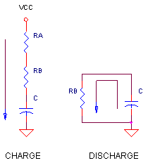
The key external component of the astable timer is the capacitor. The astable function can be distilled into just this: charge a capacitor, discharge a capacitor, ..., repeat indefinitely. How is this charging / discharging accomplished? Through resistors connected either to VCC or GND.

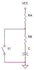
Now, we need a method to switch between the charging and discharging states. A switch will do nicely.

Switch OFF → Charge C, Switch ON → Discharge C.
The only question remaining is when do we turn the switch ON and OFF? Let's pick two voltage thresholds for the capacitor, say 1/3 and 2/3 of Vcc. The idea now is to charge and discharge the capacitor between these two thresholds. Charge C until Vc reaches + 2/3∙Vcc, then turn S1 ON. Discharge C until Vc reaches + 1/3∙Vcc, then turn S1 OFF. The two states are summarized here.
| State | Switch | What happens? | How? | Time Required |
| 1 | OFF | Charge C from 1/3 to 2/3 Vcc | RA+RB to Vcc | 0.693∙(RA+RB)∙C |
| 2 | ON | Discharge C from 2/3 to 1/3 Vcc | RB to GND | 0.693∙ (RB)∙C |
The last column shows the time for charging and discharging. To get the total oscillation period, just add the two.
Tosc = 0.693∙(RA+RB)∙C + 0.693∙(RB)∙C
= 0.693 ∙ (RA + 2∙RB) ∙ C
THE 555 TIMER
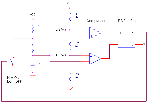
Shown as a block diagram, here's the 555 Timer. The external components are RA, RB and C. The remaining circuitry resides inside the IC.

The last piece of the puzzle is a mechanism to turn the switch ON or OFF. This is handled by resistor divider R1-R3, Comparators 1 and 2, and an RS Flip-Flop. The upper or lower comparator simply generates a positive pulse if Vc goes above 2/3 Vcc or below 1/3 Vcc. And these positive pulses either SET or RESET the Q output - turning S1 ON or OFF.
THE 555 SPICE CIRCUIT
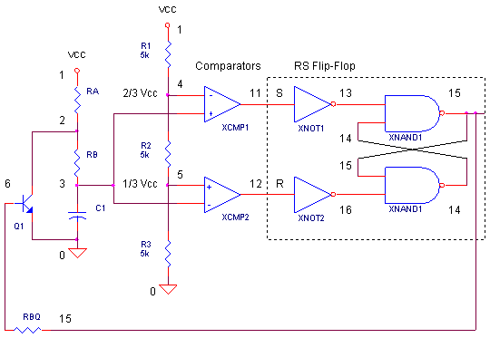
The SPICE circuit (top figure) looks almost identical to the block diagram. Transistor Q1 is called on stage as the switch. The RS-Flip Flop is played by the classic cross-coupled NAND gates. These gates are implemented using simple SPICE switches (See Basic Digital Gates). Let's start up this circuit. Later we can look under the hood of some of the SPICE models.
CIRCUIT INSIGHT Run a simulation of the SPICE file 555_TIMER1.CIR. Check out the capacitor voltage V(3) and output V(15). This output serves as both the Q1 drive and the digital output. Ahhh, just sit back and watch V(3) rising and falling exponentially towards its thresholds. To see the positive pulses created by the comparators, plot V(11) and V(12).
HANDS-ON DESIGN Pick a new value for C1 that's 1/2 or 2 times the initial value. Run another simulation and plot V(3). Initially RA = 1 k and RB = 10k. This makes for a reasonably symmetric waveform because C1 charges through RA + RB = 11k and discharges through RB = 10 k. To skew the symmetry, change the timing components to values like RA = 15k and RB = 5k, creating charge and discharge resistances of 20 k and 5 k. Test drive the timer and check out its less than symmetric waveform.
CIRCUIT INSIGHT Regarding the timing equation, you may have noticed Vcc is absent from it! Why? The exponential waveshape is independent of supply voltage. And the thresholds, derived from voltage divider R1-R3, scale with the supply levels. The beauty of these features is an oscillator that's (largely) independent of Vcc. Crank Vcc up and down to levels like 6 and 4 V. Is there any major effect on the timing?
RS FLIP-FLOP
Although the RS Flip-Flop can be modeled in many ways, the classic cross-coupled NAND gate defines this function. Furthermore, the NANDs were created from simple switches so running the SPICE file does not require a mixed-mode (analog / digital) simulator.
CIRCUIT INSIGHT Notice, the NAND and NOT gates include a small capacitor to delay the output slightly. Without this, SPICE would freeze up as it tried to calculate the transient solution. Need proof? Remove the capacitors in the subcircuits by placing an "*" before the CL statements. Run a simulation and watch what happens.
(NOTE: For the LTSPICE schematic, an RS Flip-Flop is available as a single Digital part.)
COMPARATOR MODEL
Three sections make this simple comparator: differential input, low-pass filter and output limiting. EDIFF implements the differential comparison and hysteresis functions.
EDIFF 3 0 VALUE = { V(1) - V(2) + V(5)/500 }
Hysteresis helps the comparator output switch quickly, even with slow moving inputs. As you can see, it feeds a fraction of the output V(5) to the input helping it swing faster through the threshold. Low-pass filter, RP1 and CP1, adds delay to the device. Without it, SPICE may sputter and grind to a halt when calculating the transient response. Lastly, the TABLE function creates the output limiter: V(4) = 5V for inputs > 1 mV; V(4) = 0V for inputs < -1 mV. For inputs between -1 mV and +1 mV, V(4) is a linear function between the points defined by the table.
SIMULATION NOTE
Good news; bad news. The good news is that this SPICE file accomplishes two goals: 1) show the inner workings of the 555 timer and 2) run in the limited component demo versions. The bad news is that the model may not include all of the 555 features like the reset pin and output pin drive. A forced economy of parts required a few behaviors to be left out. Also, the simple digital gates and comparators may not accurately duplicate some of the finer timing parameters.
One final note - to help our circuit start, we set the initial voltages of the capacitor and flip-flop outputs by the statement .IC V(15)=0V V(14)=5V V(3)=0V. and add UIC (Use Initial Conditions) to the TRAN command.
Learn more about functions like VALUE and TABLE in Analog Behavioral Modeling. Review SPICE Subcircuits at the SPICE Basics page.
SPICE NETLIST
Download the file or copy this netlist into a text file with the *.cir extention.
555_TIMER1.CIR - ASTABLE MODE
*
VCC	1	0	5V
*
* EXTERNAL TIMING COMPONENTS
RA	1	2	1K
RB	2	3	10K
C1	3	0	100PF
*
* DISCHARGE TRANSISTOR
Q1	2 6 0	QNOM
RBQ	15	6	15K
*
* 1/3 AND 2/3 VCC DIVIDER
R1	1	4	5K
R2	4	5	5K
R3	5	0	5K
*
* COMPARATORS
XCMP1	3 4 11 COMP1
XCMP2	5 3 12 COMP1
*
* RS FLIP-FLOP
XNOT1	11 13 1 NOT
XNOT2	12 16 1 NOT
XNAND1	13 14 15 1	NAND
XNAND2	15 16 14 1	NAND
*
* SUBCIRCUITS AND MODELS ***********************************
*
.SUBCKT NAND 1 2 3 4
* TERMINALS A B OUT VCC
RL	3	4	500
CL	3	0	10PF
S1	3 5	1 0 	SW
S2	5 0	2 0 	SW
.ENDS
*
.SUBCKT NOT 1 3 4
* TERMINALS A OUT VCC
RL	3	4	500
CL	3	0	10PF
S1	3 0	1 0 	SW
.ENDS
*
*
.SUBCKT COMP1  1 2 5
* TERMINALS: 1-INPUT+, 2-INPUT-, 5-OUTPUT
* DIFF AMP WITH HYSTERESIS
EDIFF	3	0	VALUE = { V(1) - V(2) + V(5)/500 }
* LOW-PASS FILTER
RP1	3	4	200
CP1	4	0	100PF
* LIMITER
EOUT	5	0	TABLE {V(4)} = (-1MV 0V) (1MV, 5V)
.ENDS
*
*
.MODEL	SW	VSWITCH(VON=3 VOFF=2 RON=10 ROFF=100K)
.model	QNOM	NPN(BF=100)
*
* ANALYSIS *************************************************
.TRAN 	0.05US  5US UIC
.IC V(15)=0V V(14)=5V V(3)=0V
*
* VIEW RESULTS *********************************************
*.PRINT	TRAN 	V(3) V(14)
.PROBE
.END
LTSPICE SCHEMATIC
Download the LTSPICE Schematic file Right-Click "Save file as..."
Open file in LTSPICE, hit RUN and then add Plot Panes and Traces. You'll find this version takes advantage of LTSPICE's built-in model of an RS Flip-flop.