Source Measure Unit (SMU)
Zener Diode Test
How Can You Verify If the Device Meets Spec?
Download SPICE Netlist or LTSPICE
Schematic
Right Click on filename, select "Save link as..."
Suppose you've been asked to test a zener diode given only its
datasheet! How will you design the tests given your SMU?
The answer lies in the datasheet's parameters and conditions. You'll
configure some hands-on SPICE simulations to see if a 2.7V Zener Diode will fall into
the PASS or FAIL bin.
Get a refresh of the SMU Circuit
Back to the SMU Series
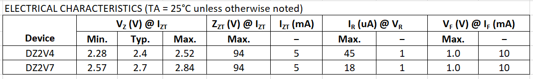
2.7V ZENER DIODE
DATASHEET
For this test, you're given a datasheet for the 2.7V 250mW Zener diode.
What's your strategy to verfiy these behaviors?
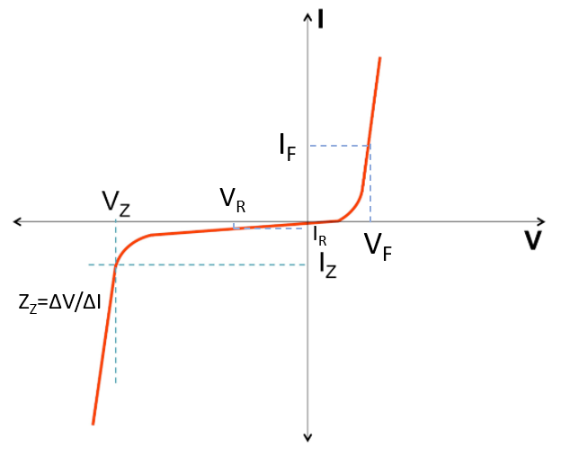
V-I PLOT
A V-I plot helps us visualize key behaviors on the zener curve.
TEST STRATEGY
How is each parameter tested? The datasheet points the way! For example, the Zener Voltage is specified as
VZ @ IZ
Which is simply a short-hand notation for
Measure Parameter @ Force Condition
Let's create four tests from the datasheet specifications.
ZENER VOLTAGE
Voltage in the reverse breakdown region.
Force Conditon FI = -5 mA Measure Parameter MV Check Test Limits if 2.57V < | MV | < 2.84V
then PASS, else FAIL
REVERSE LEAKAGE
Leakage current in the reverse region before breakdown.
Force Conditon FV = -1V Measure Parameter MI Check Test Limits if | MI | < 18uA
then PASS, else FAIL
FORWARD VOLTAGE
Forward voltage acting as a typical diode.
Force Conditon FI = +10 mA Measure Parameter MV Check Test Limits if | MV | < 1.0V
then PASS, else FAIL
ZENER IMPEDANCE
The effective resistance in the reverse breakdown region.
Z = ΔV/ΔI
= (MV2 - MV1)/(FV2 - FV1)
where MV1 is the zener voltage measured previously at FI1 = -5mA.
Force Conditon FI2 = -6mA Measure Parameter MV2 Check Test Limits Calc Z = (MV2-MV1)/(FI2-FI1)
if | Z | < 94 ohms
then PASS, else FAIL
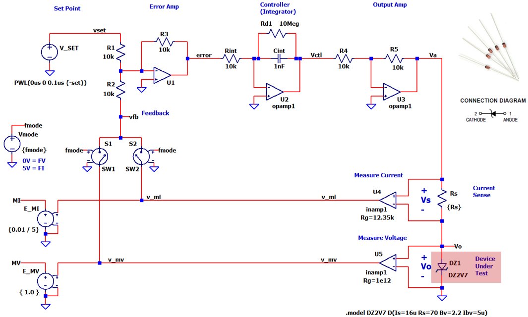
SMU CIRCUIT
Here's a quick overview of the operating ranges of the SMU circuit:
- Vrange = +/-5V,
- Irange = +/-10mA
- Current Sense
- Rs = 100
- Vs = +/-1V Max
- Internal voltage range for feedback loop.
- Vset = +/-5V (5V or 10mA Range)
SIMULATION
The diode model parameters represent a 2.7V Zener.
- .model DZ2V7 D(Is=16u Rs=70 Bv=2.2 Ibv=5u)
Each of the four tests is defined by its own PARAM statement.
- FORWARD VOLTAGE
.param fmode=5V FI=0.01 set=FI/0.01A*5V Rs=1k
- ZENER (REVERSE) VOLTAGE
.param fmode=5V FI=-0.005 set=FI/0.01A*5V Rs=1k
- LEAKAGE CURRENT
.param fmode=0V FV=-1V set=FV Rs=1k
- ZENER IMPEDANCE
.param fmode=5V FI=-0.006 set=FI/0.01A*5V Rs=1k
Enable the relevant PARAM before running each test.
- SPICE Netlist: Remove the "*" before the PARAM statement. All others add "*" at beginning of statement.
- LTSPICE Schematic: Right-click the statement and select DIRECTIVE. All others select COMMENT.
Run a TRAN simulation of SMU-FVFI-ciruit-zener-1.cir (or *.asc) with the proper PARAMs for each test below. Add trace v(mv) and then v(mi) in a separate window.
FORWARD VOLTAGE Set the .PARAMs for the Zener Voltage Test. After the current settles to FI = 10mA, read the zener voltage v(mv). Does the result fall within the datasheet limit? | MV | < 1.0V
ZENER VOLTAGE Set the .PARAMs for the Zener Voltage Test. After the current settles to FI = -5mA, read the zener reverse voltage -v(mv). Does the result fall within the datasheet limits? 2.57V < | MV | < 2.84V
REVERSE CURRENT Set the .PARAMs for the Reverse Current Test and run a TRAN simulation. After the voltage settles to FV = -1V, read the current voltage -v(mi). Does the result fall within the datasheet limit? | MI | < 18uA
ZENER IMPEDANCE Set the .PARAMs for the Zener Impedance Test and run a TRAN simulation. After the current settles to FI = -0.006A, read the voltage v(mv) as MV2. Now calculate the Zener Impedance (Resistance) as using Zener Voltage result above as MV1.
Z = ( MV2 - MV1 ) / ( 6mA - 5mA )
Does the result fall within the datasheet limit? | Z | < 94 ohms
BAD DEVICE
A 3.3V Zener Diode has been manufactured with one or more defects! Your mission is to answer - which specs FAIL?
Replace the diode DZ2V7 with DZ3V3 in the Zener Diode DZ1
- DZ1 Vo 0 DZ3V3
- .model DZ3V3 D(Is=10u Rs=90 Bv=2.81 Ibv=3u)
Run the four tests using the 3.3V Specs in the datasheet at top!
Can you find which specs for this device fail?
SPICE NETLIST
Download SPICE Netlist or LTSPICE
Schematic
Right Click on filename, select "Save link as..."
* SMU-FVFI-circuit-zener-1.cir
*
* Parameters
*
* Zener Voltage
.param fmode=5V FI=-0.005 set=FI/0.01A*5V Rs=100
*
* Forward Voltage:
*.param fmode=5V FI=0.010 set=FI/0.01A*5V Rs=100
*
* Reverse Leakage
*.param fmode=0V FV=-1.0 set=FV Rs=100
*
* Zener Impedance
*.param fmode=5V FI=-0.006 set=FI/0.01A*5V Rs=100
*
*
* Set Point
V_SET vset 0 PWL(0us 0 1us {-set})
*
* Error Amp
R1 vset  N002  10k
R2 N002  vfb   10k
R3 error N002  10k
XU1 N002 0 error opamp1
*
* Controller (Integrator)
Rint N001  error 10k
Cint Vctl  N001  1nF
Rd1  Vctl  N001  10Meg
XU2  N001 0 Vctl opamp1
*
* Output Amp
R4  N003   Vctl  10k
R5  Va     N003  10k
XU3 N003 0 Va opamp1
*
* Current Sense
Rs  Va     Vo   {Rs}
*
* Device Under Test
DZ1  Vo 0  DZ2V7
.model DZ2V7 D(Is=16u Rs=70 Bv=2.2 Ibv=5u)
.model DZ3V3 D(Is=10u Rs=90 Bv=2.81 Ibv=3u)
*
* INST AMP MI
XU4  Vo Va v_mi  inamp1 Rg=12.35k
*
* INST AMP MV
XU5  0 Vo  v_mv  inamp1 Rg=1e12
*
* Force Mode
Vmode fmode 0 {fmode}
*
* Feedback Mux
S1  v_mv vfb   fmode 0   SW1
S2  v_mi vfb   fmode 0   SW2
*
* Measure Voltage and Current
E_MV  MV 0  v_mv 0  { 1.0 }
E_MI  MI 0  v_mi 0  {0.01 / 5}
*
* Simulation
.tran 200us
*
* Opamp Model ******************************
*  pin order      in- in+ out
.SUBCKT OPAMP1    1  2   3
EGAIN     3 0   2 1     1000K
.ENDS
*
* Inst Amp Model **************************
*  pin order      in- in+ out
.SUBCKT INAMP1    1  2   3
EGAIN     3 0    value={ (V(2)-V(1)) * (1+49.4k/Rg) }
.ENDS
*
* Switch Models **************************
.model SW1 SW(Ron=1 Roff=1Meg  Von=0V Voff=5V )
.model SW2 SW(Ron=1 Roff=1Meg  Von=5V Voff=0V )
*
.end
Back to SMU Series